• 35, 1st Main Rd, Munireddy layout, Bandepalya, Garvebhavi Palya, Bengaluru, 560068

Social

Lessons from Ford vs Ferrari

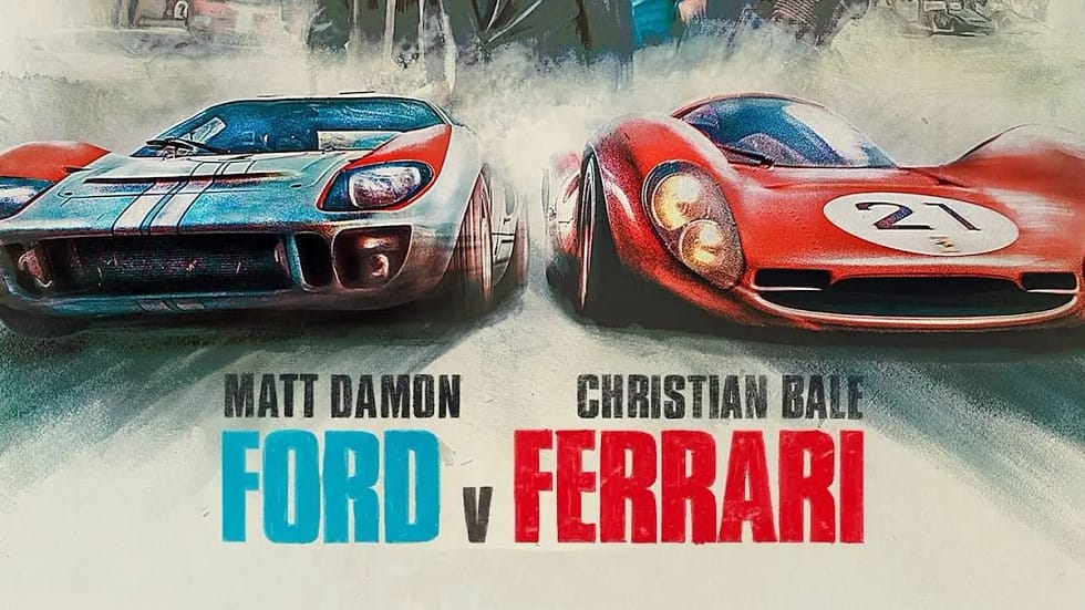
The 2019 film Ford v Ferrari, starring Christian Bale and Matt Damon, can be called a racing movie, or a David versus Goliath movie, or a mismatched buddy movie. As an entrepreneur, I saw it as all of those – but I also saw it as a movie with lessons about how the perspective of management has to change and adapt as a business grows from a startup with a prototype to an established production enterprise.

The movie tells, in a fictionalized recounting of history: how, in 1963, the Ford Motor Company begins its pursuit of an audacious and near-impossible goal.

Ford v Ferrari Poster

Ford v Ferrari is an entertaining movie with valuable lessons

Henry Ford II is dissatisfied with the state of the company his grandfather founded, and wants to shake things up. Young hotshot executive Lee Iacocca comes up with an idea: acquire Italian car giant Ferrari and its famous stable of hand-crafted marques. Ford isn’t enthusiastic, but allows Iacocca to make the approach.

Enzo Ferrari doesn’t want to sell his company, and says so with some rather creative and colourful insults. Infuriated, his pride hurt, Henry Ford II seeks revenge. He declares that Ford will defeat Ferrari at the prestigious, brutal La Mans 24-hour car race – a race that no American car has ever won.

He hires Shelby Carroll (Damon), a former champion racer and now car builder, and Ken Miles (Bale), a hotheaded engineer and driver. The movie recounts how they went all out to design, build and finally race a car that would win at La Mans and restore Ford’s wounded pride.

Though the movie title is Ford v Ferrari, the rivalry between the two is really just the catalyst that sets the plot in motion. The story is really about the two mavericks, Shelby and Miles, and their experiences working with the Ford Motor Company as they develop the world-beating car that Henry Ford II demands. Both men are creative, open to experimentation, and have hands-on experience of how races – and racecars, and drivers – operate. Their confrontation is not with Ferrari, but the ‘company men’ of Ford: the men who adhere to the corporate way of doing things because they are convinced that the tried and tested processes and procedures are the best.

In a memorable scene, Shelby’s proposal, in a red binder, goes through fully fifteen mid-level managers around the Ford HQ. All of them are cautious, reliable, trustworthy, solid and intelligent men. But this is an unprecedented project with a high degree of uncertainty – i.e., a prototype.

Shelby was a racing driver before he became a car designer and builder, and instinct honed by years of experience tells him what needs to happen for the project to succeed. How does he know? He just does. But the mindset of Ford’s middle management is different. This, after all, is the place where mass production was perfected. What they want is reliable, repeatable, structured and iterative answers – in a word, predictability.

This scene beautifully illustrates the contrast between the mindset required for prototyping – flexible, creative, willing to trust that years of experience can speed up decision-making to the point where it almost seems like a miracle of intuition – and that required for production, where it is vitally important for every stage and step to be carefully planned, executed, supervised and documented.

Both perspectives are important to the success of any entrepreneurial effort. Shelby and Miles, however brilliant they were, would have been very unlikely to beat Ferrari at La Mans without the money, facilities and production power of the mighty Ford Motor Company at their backs. When they want something done, it gets done because the company has the muscle to get it done. At the same time, Ford would not (and historically, did not) have much success building a La Mans-winning car without the experience and experimental, creative attitude of Shelby and Miles. The company struggled to solve the basic challenge of keeping the car moving for 24 hours without overheating or catching on fire.

The movie shows that being flexible and open to new ideas, adapting and pivoting as needed is a vital attribute of management when developing prototypes and new answers to challenges. Once the solution is determined, making it consistent and repeatable demands the rigour and discipline of the production mindset. The wise manager cultivates the ability to do both – and the ability to know which one to apply in which situation.

I highly recommend Ford v Ferrari to my fellow entrepreneurs: it’s a highly entertaining movie with superb racing scenes, great acting and some very funny dialogue, and it delivers several excellent lessons about business, management and leadership that any businessperson can relate to.

Spoiler alert: 

So, did all the hard work of Shelby and Miles, and the hard lessons learned by the Ford Motor Company pay off? Yes – in 1966, the Ford GT MK II defeated Ferrari at Le Mans, and just to prove it wasn’t a fluke, they did it again the next year.


Read More

Better Waste Management

Modern manufacturing practices pay close attention to their environmental impact. Failure to do so has legal and regulatory implications as well as marketing ones: suppliers’ ‘green’ credentials are frequently a criterion for selection.

The electronics industry – and the PCB industry in particular – uses many metals and processes that create large quantities of ecologically harmful waste. Some metals are dangerous if not disposed of properly, and many that can be reused are often squandered in landfills due to poor waste management practices.

Better Waste Management Practices are the need of the hour

Waste in the PCB industry

A number of materials go into the assembly of a PCB. Most PCBs use resin epoxy, phenolic resin, fibreglass and copper foil. Depending on the complexity of the circuitry in the design, metals including copper, aluminium and iron, and several alloys, may be used. At the end of its life, a PCB that is discarded means those metals and alloys go to waste.

On average, a PCB contains approximately 70% non-metallic and 30% metallic material: organic materials, chemical residuals, heavy metals and high-grade precious metals including palladium, silver, gold and copper. It is estimated that up to 7% of the world’s gold supply may be found in e-waste.

But it is not just the product itself that contains potentially wasted value. A great deal of waste is generated during the manufacturing process itself. For example, during production a PCB must be rinsed several times, leading to water contamination by chemicals and metals, and the release of some acidic emissions into the air.

In February 2003, the European Union issued the Restriction of Hazardous Substances Directive, or RoHS. This directive states that PCB manufacturers wishing to operate in or sell to EU entities may not use six hazardous substances in any stage of their production process – lead, mercury, cadmium, hexavalent chromium, and the fire retardants polybrominated biphenyls and polybrominated diphenyl ether. As the EU is a large and influential market, over the years, PCB production around the globe has begun to comply with the RoHS regardless of where the customer is.

Also in 2003, the first WEEE (Waste Electrical and Electronic Equipment) Directive was introduced, regulating the recycling of electronic waste. Under WEEE, companies that manufacture, distribute or sell electrical and electronic equipment have an obligation to treat it responsibly.

The WEEE became more stringent in 2008 and the RoHS in 2011, increasing the amount of e-waste that is required to be treated and reducing the amount that can be disposed of.

How can waste be reduced?

There are several methods by which PCB manufacturers can address the challenge of managing their waste and minimizing their environmental impact.

Product substitution.

Several alternatives may be substituted for harmful items, especially for supplementary processes like packaging, where sustainable materials are available, which can make an immediate impact on the quantum and composition of waste, and which are relatively easily to obtain and adopt.

Replacement of hazardous materials.

 In advanced manufacturing, new techniques, tools and materials are being introduced all the time. For example, when cleaning and preparing PCB surfaces, changes to the materials used, the safety precautions taken and the processes themselves can yield significant results. By using abrasive cleaning and non-chelated materials, manufacturers can reduce the amount of hazardous waste produced. A cascade cleaning system cuts down on the generation of nitric acid as a waste product. It should be noted that cascade systems are not new – for several decades, they have been used to clean machine parts in the heavy electrical industry. Customizing cascade systems for PCB manufacturing is a logical next step.

Material reuse or recycling. 

Some of the materials used in the production of a PCB can be put back into the production process. Copper from the edge, tin and lead-tin from the solder dross are examples of this. By reusing parts, the process also uses less water. Copper oxide can be used to reduce the reliance on copper hydroxide, which is harmful to the human respiratory system.

Material recovery and segregation.

 By joining in or setting up a well-thought-out recycling process, manufacturers can turn waste back into raw material, or supplement their earnings by selling their recovered materials to other industries. Alloys and metals are valuable and can be reused several times, reducing the amount of waste generated and the PCB manufacturer’s dependence on being able to source new materials on time and at the right price.

Traditional PCB recycling involves dismantling the boards, crushing them and physically separating them using magnetic or high-voltage electrostatic methods. This approach is relatively cheap and enables the recovery of metallic components, though it does not solve the problem of segregating heavy metal elements from high-grade precious metals.

Thermal or chemical recycling can obtain purified metals, is much more efficient and has the potential for a much greater economic return. However, the high processing temperatures or high-pressure requirements can cause hazardous fumes, thus creating a new problem while resolving the existing one.

Podrain has tied up with a reliable, pollution control board certified partner for waste disposal. We also return materials and components (unused or even partially working) to our customers so that they can be reused at their end.

We value sustainability and even if we move to an inventory led model we will hope to find solutions that will continue to keep our manufacturing sustainable. 

Read More

Factory Location: How to make a choice

India

India

Entrepreneurship is all about making decisions and one of the key decisions every manufacturing entrepreneur faces is the best location and layout for the plant or factory. Should it be in a city, semi-urban or industrial area? Is proximity to an employee pool, educational centres and public transport important? What about public utilities? Taxation and incentives?  Which amenities are likely to be most vital to success?

We’ve been thinking about this at Podrain and went back to basics on it.

Plant location is a strategic decision that  is nearly impossible to change without incurring considerable losses. The ideal location is one that minimizes the cost of production, supports a large market share, maximises social benefit and eliminates risk. Locational analysis that takes into account demographics, trade area (availability of and access to customers), competitive, economic and traffic analyses and can help determine the right location.

A location in which some costs are higher may still be the best choice if it maximises net advantage, i.e., its overall unit cost of production is lowest.

Here are some things we are considering when selecting a suitable location for a factory:

  1. Natural or climactic conditions
  2. Cost of land or land lease
  3. Availability and access to raw material
  4. Transport costs – inward, to bring in raw material, and outward, to sell or distribute finished products
  5. Availability and access to market
  6. Availability and access to infrastructure – developed industrial sheds, link roads, transport hubs, public utilities, civic amenities, means of communication
  7. Availability and access to both skilled and unskilled labour, as required, and local labour rates
  8. Availability and access to banking and financial institutions
  9. Safety and security of the plant, its workers and its assets
  10. Government and regulatory environment – positive and negative incentives, including cheaper utilities, tax relief, liberal local labour laws, pollution control and waste disposal regulations, among others
  11. Personal reasons, such as being close to family, familiarity with a particular place, or a network of known associates whom we can call upon for financial, operational and emotional support. This isn’t intuitive to admit but it’s really important to have a good support system.

Not all these considerations carry equal weight. For example, government incentives cannot compensate for poor public infrastructure. Running costs at a plant can contribute significantly to the overall cost of manufacturing, and poor location selection can cause a business to fail as its growth and efficiency are constrained.

MSMEs like us often do not have the financial or operational capacity to compensate for the shortcomings of public infrastructure , so our ability to adjust to an unsupportive environment is extremely low, particularly in the early stages of the manufacturing journey.

Is there something else we should include? What is your experience. Do write to us or add your comments to let us know.

Read More

Quality testing for prototypes

In PCB manufacturing, repeatability and consistent quality are critical – whether for large-scale production, small batches or prototypes.

Skilled and experienced technicians can and do create excellent work, but relying on individuals to establish, deliver and sustain top-quality results is risky. Programming Automatic Inspection Machines and processes is expensive, time-consuming and not always practicable, especially when prototyping.

Testing

Testing

Prototype QC needs to ensure that the design will work; that it is safe, and meets certain standards of quality and reliability; that it performs to expectations; and that it addresses its purpose.

Small batch PCBs have some rather unique attributes:

  • High Mix, Low Volume (HMLV). It’s likely that the PCB manufacturer builds several board designs in this environment to ensure efficient use of their production infrastructure.
  • Higher performance, reliability and quality requirements. Small batch and prototype PCBs are often intended for critical applications where more stringent IPC standards apply, like aerospace, automotive safety or medical devices. Quality and reliability expectations can be significantly higher for these critical system applications.
  • Complex designs. Prototypes are created to solve specialized and often complicated challenges, which means their designs are complex, requiring atypical manufacturing processes

How to ensure the best quality standards for prototypes and small batches

  • In-circuit testing (ICT). Provides a reliable, high-fault coverage verification method for the majority of PCB assembly electronic components that’s free of human error. It’s great for big assemblies or ball grid arrays and after assembly.
  • Short circuit testing. The main cause of PCB prototype defects is a short circuit between its larger components. For example, a fastener between two proximate pins can damage the microcontroller by triggering a short. It is vital to gauge the impedance each voltage node to the ground. Faulty components or incorrect soldering can cause components to overheat.
  • Flying probe test. A practical, cost-effective technique for prototypes and small batches that tests PCB probes from one spot to another, looking for singular issues in the circuit – shorts, capacitance, resistance, inductance, opens and problems with diodes.
  • x-ray inspection. As the prototype is being manufactured, an x-ray technician runs tests to locate defects, looking for elements that may be hard to discern with the naked eye – for example, joined connections, internal traces or barrels.
  • Functional testing. The #1 criterion for a prototype’s success is, “Does it work?” Performing a functional test requires the parameters for ‘success’ to be clearly defined. Functional testing takes a long time, because it simulates the real-life environment in which the prototype is expected to work. But in terms of long-term value, it’s worth doing. A great deal of money and time can be saved by identifying potential operational pitfalls and eliminating them at the design stage.
  • Burn-in testing. Intended to identify failures early and initiate load capacity. Burn-in testing helps identify potential dangers relating to power being pushed through the electronic components for extended periods of time. One must keep in mind that individual prototypes may be partially or even completely damaged by a rigorous burn-in test, and the test’s utility to prototype QC should be decided based on the destination application of the PCB.
  • Automated optical inspection testing (AOI). Camera-based visual inspection to identify issues that may emerge on the board during the preliminary phase of assembly. It’s wisest not to rely entirely on AOI, but to complement it with an ICT or flying probe for more accurate QC results.
  • Inverted polarity testing. The more manual assembly, the higher the risk of human error. The simple act of ensuring that each individual component is set up based on its polarity can prevent the complex and delicate components of your prototype being badly damaged. Protection diodes can protect PCBs but add to their power consumed.
  • Populated components testing. A simple BOM cross-check to ensure that the components selected fit the board design can save investigative time and effort later in the process.

Several other QC approaches, including tests for PCB contamination, solderability and peeling; micro-sectioning analysis; and time-domain reflectometers, can identify faults or be used in combination with those discussed above, like ICTs and flying probes.

Choose the right QC test(s) for your prototype

It begins with clearly defining the purpose and desired performance levels of the PCB; weighing the pros and cons of the available tests – which include costs, time required, destructive vs. non-destructive; and always keeping in mind, especially when prototyping, that the design-test loop can flex and adapt as the product design is iteratively perfected.

It’s always a good idea to partner with a manufacturer who is committed to the best quality; has documented and traceable processes; has the necessary quality and classification standard certifications; is experienced at HMLV manufacturing; and leverages technology to ensure high-quality, repeatable results.

Podrain collaborates closely with its clients when prototyping and producing small batches, and meets the highest quality and classification standards. We advise clients on the right mix of testing to ensure that their prototype PCBs meet the final test of quality – sustained, reliable, top-level performance in the field.

Read More

Why We Need to Near Source Electronic Components

Why we need to Near Source Electronic Components

The past two years have offered some harsh lessons to all in the PCBA industry on the value of inputs. For a long time, the cost paid was the only consideration. The supplier might be located on the other side of the world, but if the cost was marginally lower, the choice was clear. But the pandemic changed all that. The cost of logistics / transport that used to be negligible ballooned beyond expectations. And for some parts – no matter what cost we were willing to pay – the availability just did not exist.

PCB Assembly

PCB Assembly

In India, we import more than 90 percent of the components required for assembling PCBs locally. These imports come from 4 countries – China, Taiwan, Vietnam, and Malaysia. A break down at one source country, as we saw in 2020 and 2021, drives up the cost of doing business for all.

Here’s our experience with supply trends for some of our major inputs:

Bare PCBs:  

Bare PCBs are the stronger point in our supply chain. We have seen reliable suppliers of Bare PCBs based in Tamil Nadu and in Gujarat. We (and many of our customers) have been able to source Bare PCBs in the past 18 months with no major issues. Supply lead times have remained consistent and price increases have stayed within tolerable limits.

Assembly Machinery: 

Machinery needed for PCBA is mostly manufactured outside India by majors like Yamaha, Fuji, Panasonic, and Siemens. While prices have stayed stable, lead times have increased considerably. What used to be available in 4 weeks now takes 4 months to get delivered. We’ve had to plan and order earlier than ever before for any capacity enhancements or repairs and replacements.

Other Components / Services: 

Integrated Circuits (IC’s), their component resistors, capacitors et al, solder paste etc. are mostly imported and have all seen prices and lead times zoom up. 52 weeks is now the new normal! Companies like Micron, TI, Cypress, Infineon, Latis, NXP have factories based in China, Taiwan, Malaysia, and Indonesia. When supply and manufacturing centers were shut and major ports slowed down, component shortages have visibly hit every industry from automotive to computers and mobile phones. Even stocks held by major distributors Avnet, Future, Arrow, or online suppliers like Digikey, and Mouser could not tide the industry over for long.

This is the area where India needs to attract investment and build manufacturing capacity. 

What Next:

The government has already recognised the need for building an electronics components manufacturing ecosystem. It is doing its part by offering Production Linked Incentive programs and other sops to encourage manufacture of components in India. It is now up to us in Industry to pick up the challenge and partner in building a strong local eco-system for components. 

Read More

Agritech: High-end Hardware Applications for Indian Agriculture

The global human population is projected to reach 9.8 billion people by 2050. Food security is a critical concern worldwide. Resource availability, distribution and access imbalance, higher agricultural and dairy output, and sustainability are major challenges.

The Indian agriculture sector is valued at over $370 billion. It employs 40% of the population and contributes nearly 20% of India’s GDP. Agritech is vital to ensuring our nation’s food security issues. A 2020 E&Y study estimated that the Indian agritech market could reach $24 billion in the next 4 years. Another study put the number at $35 billion.

Indian Agritech has great potential

Over 1,300 Indian startups are working in this space as of October 2021. They use AI, ML, IoT and other digital technologies to improve productivity, efficiency, revenue and profitability for farmers. In 2020, Indian agritech startups received $242 million in funding in just ten months.

These startups offer a range of products and services including sensors, signal conditioning, processing and security, power management, connectivity, and positioning. As a precision-engineering EMS manufacturer, Podrain works with IoT-driven agritech startups to create the hardware required for smart farming. Some of the many applications are:

Precision agriculture and farm management.

Geospatial and weather data, IoT sensors for humidity, temperature and other variables, resource and field management, energy and water use, and robotics on farm equipment.

Farm infrastructure and equipment.

Industrial automation using machinery, tools and robots to seed, harvest, and handle materials. Greenhouse systems, temperature and humidity monitoring, environmental controls, irrigation and water management, heating and ventilation monitoring.

Dairy farm optimisation.

IoT sensors monitor the health parameters, milk production, eating patterns and nutrition, fertility and reproductive cycle of individual cows, and overall herd health. Diseases can be detected early. Digital milk analysis devices measure fat and water content, SNF and contaminants at every stage.

Cultivation and land use.

GPS data have applications in land mapping, soil quality, crop placement, soil sampling, weed identification, determining the right time to harvest, pest management and optimum pesticide use, and water availability and irrigation, among many others.

PCBs are a foundational component of IoT-based digital technology. Podrain has vast expertise in developing customised solutions and solving highly complex problems for our clients. We apply our talents to the vital area of agritech. It presents a large and growing opportunity to harness the power of digital technology to improve the quality and quantity of agricultural and dairy output, and the economic well-being of 40% of India’s population.

Read More

Complex assemblies – some samples

Telit ME910 / LE910

Part number: ME910 / LE910
Telit ME910 / LE910
  • Part Number: ME910 / LE910
  • Make: TELIT
  • Dimensions: 28.2 X 28.2 X 2.2 MM
  • 4G LTE, CAT 1, 4
  • Mobile IoT 3GPP REL 13, 14 – LTE CAT M1, NB1, NB2 
  • 3G and 2G Series
  • Voice Capable Variants – Volte, Analog, and Digital Audio
  • Certified with Regulatory Bodies and Mobile Operators Worldwide
  • Multiple I/O
  • Optional GNSS

Digi International : CC-WMX-JN58-NE

  • Part Number: •CC-WMX-JN58-NE
  • Make: Digi International
  • Dimensions : 29mm X 29mm X 3.5mm
  • Description : Bluetooth, Wi-Fi, 802.11A/B/G/N/AC, Bluetooth v4.0 Transceiver Module 528 mhz  Surface Mount

Quectal: EG95EXGA-128-SGNS

Quectal: EG95EXGA-128-SGNS
  • Part Number: EG95EXGA-128-SGNS
  • Make: Quectel
  • Dimensions: 29mm X 25mm X 2.3mm
  • Description: Cellular, Navigation Beidou, Edge, Galileo, Blonass, GPS, GNSS, GPRS, GSM, HSPA+, LTE, UMTS, WCDMA Transceiver Module – Antenna not included Surface Mount

Telit: GE310-GNSS

Telit: GE310-GNSS

Part Number: GE310-GNSS

Make: TELIT

Dimensions: 18mm X 15mm X 2.2mm

Description:  Automated Manufacturing Process Friendly. Miniature and Futureproof footprint. BT 4.0 Transceiver. GPS, GLONASS, Galileo and Beidou navigation, Ideal solution for applications such as asset management, utilities, and telematics. Battery-friendly operation with 2.8V GPIOS.

Quectel: EG91NAFB-512-SGNS

Quectel: EG91NAFB-512-SGNS
  • Part Number: EG91NAFB-512-SGNS
  • Make: QUECTEL
  • Dimensions: 29mm X 25mm X 2.3mm
  • Description: Cellular Navigation on Beidou, Galileo, Glonass, GPS, GNSS, LTE, UMTS, WCDMA. Transceiver module- Antenna not included surface mount

Honeywell: LGA_299_35MMX35MM_BETTER_SOM

Honeywell: LGA_299_35MMX35MM_BETTER_SOM
  • Part Number: LGA_299_35MMX35MM_BETTER_SOM
  • Make: Honeywell International Inc.
  • Dimensions: 35mm X 35mm X 6mm
  • Description: SOM , I.MX6 SOLOX-2 , 4GBYTE EMMCFLASH , 1GBYTE DDR3L

New Technologies Inc: A-365-MQ-A00

  • Part Number: A-365-MQ-A00
  • Make: New Technologies Inc
  • Dimensions: 22.5mm X 15.05mm X 1.13mm
  • Description:  The A-365-MQ Fingerprint sensor is a fingerprint scanner in an LGA Style package. The sensor is based on capacitative contact technology with hardened surface and enhanced ESD immunity.
Read More

complex assemblies

Metal BGA

Electronics have become essential to daily life. Everything from refrigerators to military aircraft contains electronics. Today’s critical advanced assembly challenges mainly fall into three categories: performance, usability and productivity. To build and visualise product designs quickly and economically, engineers must address all these challenges.

On the other hand, manufacturing techniques are becoming more advanced and aesthetics are increasingly in demand. Project lifecycles and budgets are constrained. Sometimes, these constraints mean that DFM standards are overlooked in PCB design. For example, if the PCB has to fit in a box of fixed dimensions, the PCB design has to be tweaked accordingly. Or, components with different reflow profiles may be used on the same sid

Newer design houses or inexperienced engineers and designers may be prone to these mistakes. But not validating designs with tool and industry standards is bad practice. Here are just a few examples:

Pad mismatch

 If the copper termination pad separates partially or completely from the board, it can be hard to identify the fault; the pad may look intact as the solder usually remains attached to the component. The cause is usually mechanical strain that begins during testing, manufacturing, vibration while being transported or even when connectors are attached. PCB performance is impaired and performance is inconsistent. Extensive or even destructive testing may be required to positively identify the cause. Podrain follows a painstaking process to minimise the risk of damage from pad mismatch at each step.

No silkscreen. 

The silkscreen does not impact the electrical functionality of a PCB, but it is still extremely valuable as it provides essential information when assembling the PCB. It provides simple visual feedback that helps to catch deeper problems. It is not merely for aesthetic purposes. It is information that should not be separated from the board. Unique ID numbers, warning symbols, certifications etc. should be displayed on the board. At Podrain, we treat correct and comprehensive silkscreens as an integral part of the PCB.

THT vs. SMT components. 

When SMTs were developed in the 1980s they were expected to completely replace THTs. But THTs and SMTs are not always interchangeable. THTs offer reliable and useful in test and prototyping applications where frequent manual adjustments and replacements are needed. But SMTs are almost always more efficient and cost-effective. Podrain’s extensive experience in a wide range of applications gives us the expertise to know which type of components to use for a given project.

Incorrect polarity marking. 

To prevent polarised component packages from being inverted during assembly machine setup or manual soldering, accurate polarity marking is critical. It is only necessary for land patterns that have a specific rotation during assembly. Incorrect polarity markings can cause equipment damage, short-circuiting, serious injury, fires or even explosions. Podrain follows stringent Post Assembly Inspection Process protocols to visually validate that assembly insertion is done correctly

Incorrect component separation. 

Most designers are used to PCB clearance rules for spacing between traces in a single layer. However, many design houses overlook PCB clearance between layers. Today’s circuit designs often involve a single PCB with power and controls on the same substrate. This may put high-voltage traces close to low-voltage signals, creating a risk of arcing. The resulting sparks can permanently damage the port of the low-voltage component. Podrain designers and engineers keep ourselves up to date on the latest IPC-2221B design standards to ensure optimum manufacturability with minimum risk.

Podrain’s customers have brought us some interesting design challenges.

A top manufacturer of electric vehicle charging stations found that the PCBA yield was below 90%, lower than expected. The company approached Podrain to investigate. The issue was all the more challenging because the assembly was ROHS. Planning and finding the right profile, especially on a PCB that uses BGA + LGA, is an art.  By devoting our experienced people to solve this, we iterated through a range of 11 temperature profiles in a reflow oven within just 2 days to find the solution.

Another customer set us the challenge of setting the right profile for a board designed with a heavy BGA connector having multiple ceramic BGAs, including micro BGAs, on a 2mm thick PCB. The issue is these kind of connectors use very high temperature for soldering. 265 degree Celsius plus is needed for soldering but a normal BGA can tolerate only 245 to 255 degree Celsius. We designed and conducted multiple trials by changing the solder paste for each profile. After 15-20 trials supported by some fixtures, we were able to determine the best profile for the customer’s board.

Podrain has solved many such complex assembly design challenges for our customers.

Read More

The Art of Quick Turn Prototype Manufacture – Some learnings

As a PCB assembly and manufacturing unit, we face several challenges in ensuring we can meet the turnaround time our clients ask for while still delivering a quality product. This is a short post on the challenges we face and how we solve them.

6 M framework based thinking helped Podrain find solutions for quick turnaround manufacture

Managing Part Availability Delays

Every manufacturing organization has dealt with issues in this area. The critical part is held up in customs. A normally reliable supplier doesn’t have stock just now. The wrong part got shipped. The list of such issues can be long. Our clients purchase the parts for us in most cases because we are a “job-work” oriented partner, but there are many occasions when the part isn’t available on time but the end date to finish the manufacture is the same!

We’ve seen clients work hard through the day and the part reaches us at the end of the regular workday. We have adapted by having a 3 shift operation in place so that we can take up the order manufacture at any time and ensure client timelines are met. We also ensure that our strongest team members are available on the late shift. It can be tough working late at night on an important order and we put our toughest people on the job to make sure it gets done right.

There are some consumables, that we must order and here we invest in supplier relationships. Our stencil suppliers, for instance, deliver within a few hours because they know they can trust our volume commitments and payment cycles.  

Kit Condition Checks First

For larger clients who have their own kitting teams, 99% of the kits arrive in good condition and we can start manufacture immediately. However, many of our clients are startups or design houses that are still experimenting. The parts are directly shipped to us without kitting checks at the client’s end. 

We solve this by frontloading our effort in checking kits. Where other manufacturers would ask two people to run kit checks, we allocate 6 people. And we work with the client to solve for deficiencies right away – if there is a part shortfall can we run a smaller batch? Is there additional testing we can do on a smaller batch, while we wait? Is there an alternate part or source we have seen that we can connect them to? We work flexibly with our partners to ensure their goal is met.

Data Package Standardization

In the past when we accepted all client data packages as-is, we would spend a day verifying the documents – gerbers, assembly drawings, additional assembly instructions, etc. – and then mapping them to our process to ensure there were no misses. Working with our clients we realized many of them were flexible on giving us this information in a format that we requested. This saves us time and ensures we can follow a Total Quality Management process even within a 48 or 72-hour manufacturing turn. 

We’ve used the 6 M framework – Manpower, Method, Machine, Material, Milieu and Measurement to think through problems and find some of these solutions. I highly recommend this to anyone working in Manufacturing or even in other industries.  

That’s it for this month. I’ll write again with more of our learnings next month. 

If you want to know more about Podrain and our electronics manufacturing services contact us and we will get back to you at the earliest

Read More
Automotive

Increasing Share of Electronics in AUTOMOBILES

Many recent news articles have pointed out the effect of semi-conductor chip shortages on automobile output. There will be 7.7 million fewer vehicles produced and over $210 billion in revenue lost in the year 2021 according to some reports.* This has taken many consumers – who don’t realize the extent of shift in automotive technology – by surprise. 

 Cars now contain more electronics than ever and their share is only growing. According to this research report from McKinsey & Company, software and electronics have become the focus of most automotive companies.  Power Electronics, growing at 15% , sensors at 8% and ECU’s /DCU’s growing at 5% plus will drive the global size of the automotive electronics industries to $469 billion by 2030. 

At Podrain Electronics we are working with automotive OEM’s and other players as they ride the wave of change. 

Automobile OEM’s are shifting gears into electronic mode:

Automobile components that were previously electrical or mechanical systems are now getting an electronic layer.  For example, we have worked with a major Indian automotive manufacturer on the prototype “anti-pinch” window sensors for their new range of SUV’s.  The electric motor, which operates the power window is fitted with a sensor that can sense any obstacle and stops the winding action. Parents of fidgety children who like to put their hands out of a window or pets who like to stick their noses out into the breeze can drive easier, knowing this technology will keep them safer.  

This example is the tip of the iceberg. Sensors are being used in engine, power, steering, braking and acceleration systems converting automobiles from electro-mechanical machines to electronic & software devices. For examples, a tire manufacturing OEM client of ours is integrating electronics to create a Tire Pressure monitoring system that will enable them to optimize tire pressure based on weight of the load, road and environment conditions.  The ability to remotely monitor the performance of their products opens up new opportunities to provide extended support , warranties and differential pricing for them.This is only one example of an OEM whose product and commercial model are changing to suit the times. 

Fleet Management & Allied Services need electronics in automobiles: 

We have supported clients for GPS and Vehicle Tracking Systems manufacture – another growing space of automobile electronics. There are several use cases for Fleet Management Solutions. They help track on-time arrival and departure of vehicles, fuel consumption, route monitoring and modification, safety tracking etc. Fleet management solutions and Asset Tracking are often done by other businesses and not by the Original Equipment Manufacturer. According to Mordor Intelligence this will be a USD 22 billion in 2026** and we certainly expect to help many of the companies in this area. 

The future of mobiility – whether you choose a traditional fossil fuel vehicle, an electric one or a hybrid – certainly involves electronics! 

If you are looking for electronics manufacturing services support for your company contact us and we will get back to you at the earliest.

Read More