• 35, 1st Main Rd, Munireddy layout, Bandepalya, Garvebhavi Palya, Bengaluru, 560068

Social

5 Top Trends in electronic Manufacturing services

The Evolving Landscape: Top Trends Shaping Electronics Manufacturing Services

The world of electronics manufacturing services (EMS) is undergoing a dynamic transformation. 

The electronics industry is embracing new trends that are redefining how electronic products are designed, produced and delivered. This is being fueled by technological advancements, globalization and ever-evolving consumer demands.

This blog delves into the key trends shaping the EMS landscape, equipping you with insights into the future of electronics manufacturing.

1.  The rise of Generative AI and robotics in manufacturing

Industry 4.0 is bringing a new generation of autonomous robots that are programmed to do specific tasks without human intervention. These include mobile robots for pick and place operations and inventory scanning drones. They are equipped with advanced software, machine vision, AI and sensors and are able to perform highly complex and delicate tasks taking inputs from their environment. Read more about it here. In our previous blog we covered how Generative AI is transforming the electronics manufacturing industry.  

Generative AI is transforming the areas of Digital Twins, Supply Chain, Predictive Maintenance, Customer Support and PCB design. 

Generative AI in Electronic Manufacturing

2. The Internet of Things (IoT) Revolutionizing Manufacturing

The integration of IoT devices and sensors into production lines is transforming EMS. These connected devices collect real-time data on equipment performance, resource utilization, and environmental conditions. This data empowers EMS providers to gain deeper insights into their operations, enabling predictive maintenance, reducing downtime, and optimizing production efficiency. In addition, IoT-enabled equipment facilitates remote monitoring and control, allowing for greater flexibility and adaptability in manufacturing processes.

IOT

3. Sustainability Takes Center Stage

Environmental concerns are driving a growing focus on sustainable manufacturing practices within the EMS industry. Consumers are increasingly demanding eco-friendly products and responsible production processes. EMS providers are responding by adopting sustainable sourcing of materials, implementing energy-efficient technologies, and minimizing waste through recycling initiatives. For example, design-for-environment (DfE) principles are being integrated into product development to create products that are easier to disassemble, recycle, and reuse at the end of their lifespans.

Sustainability

4. Advanced Materials and Miniaturization: Pushing the Boundaries

The relentless pursuit of smaller, more powerful electronics is driving innovation in materials science. EMS providers are exploring new materials like graphene and nanomaterials that offer unique properties, enabling the development of lighter, more energy-efficient, and high-performance electronic components. In addition, miniaturization techniques are allowing for the creation of increasingly compact and complex electronic devices, paving the way for a new generation of innovative products.

Miniaturization

5. 3D Printing and Immersive Technologies: Redefining Manufacturing

3D printing is transforming the way electronic components are manufactured. This technology allows for rapid prototyping, on-demand production, and the creation of complex geometries that are difficult or impossible with traditional manufacturing techniques. While 3D printing may not yet be suitable for mass production, it offers immense potential for customization, low-volume production runs, and the development of innovative new electronics. Likewise, immersive technologies like Virtual Reality (VR) and Augmented Reality (AR) are being explored for training purposes, remote collaboration, and visualizing product designs within the EMS industry.

The Road Ahead: Embracing Change and Innovation

The future of EMS is bright, fueled by continuous innovation and a commitment to meeting evolving customer needs. By embracing these emerging trends, EMS providers can ensure they remain competitive in a rapidly changing landscape. The key lies in adaptability, a focus on sustainability, and a willingness to invest in new technologies that will shape the future of electronics manufacturing.

 Download our brochure here.

Read More

How an EMS can supercharge your PCB Prototyping

Introduction

Mounting demand for consumer electronics like mobile phones and wearable technologies, IoT and automobile electronics is driving corresponding demand for EMS. The Electronic Manufacturing Services market was valued at 580 billion in 2023, growing at a CAGR above 5% between 2024 and 2032 according to Global Market Insights. EMS can supercharge your PCB prototyping.

In this exciting world of electronics development, transforming your innovative ideas into a tangible prototype is a crucial step. While the process can be exhilarating, navigating the complexities of PCB (Printed Circuit Board) prototyping can also feel daunting. This is where partnering with an 
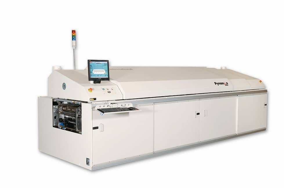
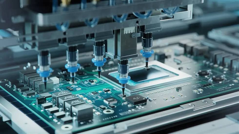
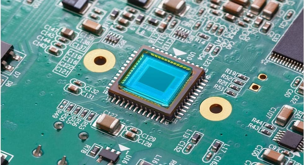
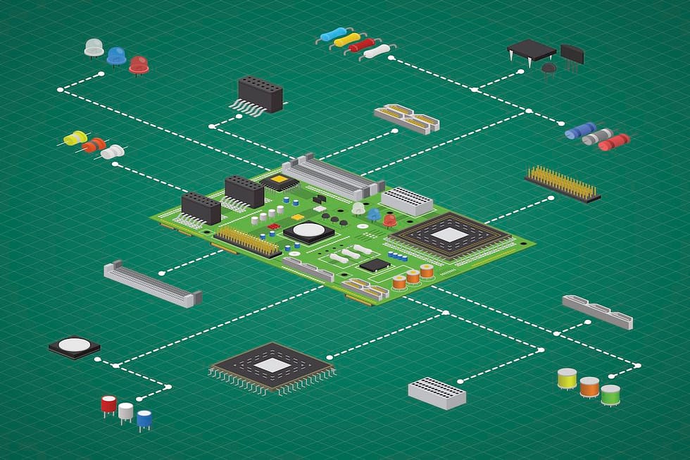
Electronic Manufacturing Services (EMS) provider can be a game-changer.

EMS. for PCB prototyping

Why Consider an EMS for PCB Prototyping?

Here are some compelling reasons to leverage an EMS for your PCB prototyping needs:

  • Expertise and Efficiency: EMS providers possess extensive knowledge and experience in PCB design, fabrication, and assembly. Their expertise can help you avoid costly design errors and ensure your prototype meets all functional and quality standards. Additionally, their established production processes streamline the prototyping journey, saving you valuable time and resources.
  • Advanced Technologies: Modern EMS providers are equipped with cutting-edge technologies like high-density interconnect (HDI) capabilities and advanced surface mount technology (SMT). This allows them to fabricate complex PCBs with intricate features, ensuring your prototype accurately reflects your final product design.
  • Quality Control and Testing: Maintaining high-quality standards is paramount during prototyping. An EMS partner offers access to sophisticated quality control measures and testing procedures. This ensures your prototype functions flawlessly and adheres to industry specifications.
  • Reduced Costs and Improved Time-to-Market: While the initial investment might seem higher, partnering with an EMS for prototyping can ultimately save you money. Their efficient processes and bulk purchasing power often translate to cost savings on materials and components. Furthermore, their expertise can help you avoid design iterations and delays, accelerating your time-to-market.

What to Consider When Choosing an EMS Partner for Prototyping

  • Experience and Capabilities: Select an EMS with a proven track record in prototyping PCBs similar to yours in terms of complexity and functionality. Ensure they have the necessary technology and expertise to handle your specific requirements.
  • Communication and Collaboration: Effective communication is vital. Choose an EMS partner that fosters open communication and actively collaborates with you throughout the prototyping process.
  • Turnaround Time and Budget: Clearly define your project timeline and budget expectations upfront. Choose an EMS that can deliver high-quality prototypes within your timeframe and at a cost that aligns with your budget.
Podrain Electronics

Partnering for Success: A Symbiotic Relationship

Working with an EMS for PCB prototyping fosters a symbiotic relationship. You contribute your innovative ideas and design expertise, while the EMS provider brings their experience, technology, and streamlined processes. This collaboration empowers you to bring your vision to life faster and with greater efficiency, paving the way for a successful product launch.

Ready to Take the Plunge?

By understanding the benefits and considerations involved in partnering with an EMS for PCB prototyping, you can make an informed decision. With the right partner by your side, you can navigate the exciting world of electronics development with confidence, transforming your ideas into reality.

At Podrain we specialize in prototype manufacturing. We have been in the prototype manufacturing business for the last 7 years. We have a very experienced team who have been in the EMS business for over a combined 40 years. We pride ourselves on our service and on-time delivery. We cater to startups specializing in IoT, healthcare, defense and aerospace. Our facility is an extension for a lot of design house to build the first boards and complete their initial testing. We have state of the art equipment for assembly, inspection and testing. We also invest in quality assurance and we have received ISO 9001:2015 and AS9100D certificate. We offer job work as well as turnkey assembly services.  Download our catalog of services here.

Read More

Generative AI in Electronics Manufacturing

The electronics manufacturing industry is a powerhouse of innovation, constantly pushing the boundaries of miniaturization, performance, and efficiency. But in this ever-competitive landscape, manufacturers are seeking new ways to optimize processes, reduce costs, and accelerate product development. Enter generative AI, a revolutionary technology poised to transform the electronics manufacturing landscape. In this blog you will learn how Generative AI can be used in electronics manufacturing.

Generative AI, unlike traditional AI focused on analysis, excels at creating entirely new data or content. This unique ability unlocks a treasure trove of possibilities for electronics manufacturers.

PCB Assembly Facility

Revolutionizing Quality Control

Flawlessly inspecting intricate electronics components is a significant challenge. Generative AI can create vast amounts of synthetic data depicting various defects on PCBs (Printed Circuit Boards). This data can then be used to train deep learning algorithms for visual quality inspection (VQI) systems. These AI-powered systems can identify even the subtlest anomalies with superhuman accuracy, significantly improving product quality and reducing scrap rates. . Landing AI is a company that makes building Computer Vision applications using Generative AI very easy.

Predictive Maintenance for Maximum Uptime

Unplanned equipment downtime can cripple production schedules and eat into profits. Generative AI can analyze sensor data from machines to identify subtle patterns that signal potential failures. By predicting these issues before they occur, manufacturers can schedule proactive maintenance, minimizing downtime and maximizing equipment lifespan. Read about the 100 top predictive maintenance companies here. 

Generative AI Visual Inspection
Visual Inspection for Quality Control
Generative AI Preventive Maintenance
Preventive Maintenance

Optimizing the Power of Digital Twins

Digital twins, virtual replicas of physical systems, are becoming increasingly valuable for electronics manufacturers. Generative AI can take digital twins a step further. By creating realistic simulations of various production scenarios, manufacturers can identify bottlenecks, test new configurations, and optimize production processes without ever disrupting the actual assembly line.

Jensen Huang the CEO of Nvidia mentioned Digital Twins as one of the key use cases of AI in manufacturing in his keynote at GTC 2024. You can read about what Nvidia is doing to enable Digital Twins here.

Design Innovation at Warp Speed

The traditional product design process can be slow and iterative. Generative AI can act as a powerful design assistant. By analyzing existing product data and user preferences, generative AI can suggest entirely new design concepts or variations, accelerating innovation and helping manufacturers bring products to market faster.

Digital Twin
Digital Twin
Generative AI Design Innovation
Design Innovation

A New Era of Supply Chain Management

The complex and dynamic nature of electronics supply chains can lead to disruptions and shortages. Generative AI can analyze historical data and market trends to predict potential supply chain issues. This foresight allows manufacturers to proactively secure critical components and adjust production plans, ensuring a smooth flow of materials and a timely delivery of finished products.

The Generative AI Advantage

Beyond these specific use cases, generative AI offers several advantages for electronics manufacturers:

  • Increased Efficiency: Generative AI automates tasks, streamlines processes, and optimizes decision-making, leading to significant efficiency gains.
  • Reduced Costs: Improved quality control, predictive maintenance, and optimized production processes all contribute to substantial cost savings.
  • Enhanced Innovation: Generative AI accelerates product development and fosters a culture of innovation within manufacturing teams.
  • Improved Sustainability: By optimizing resource utilization and minimizing waste, generative AI can contribute to more sustainable manufacturing practices.
Read More

Factory Layout – What are the Options

In my previous post we covered what to consider for factory location. Having selected a location in which to set up a factory, the next question is how to lay it out.

Factory layout refers to the arrangement of physical facilities so as to have the quickest flow at the lowest cost and with the least amount of handling in processing from the receipt of material to the dispatch of the finished product. The aim is to allocate and arrange space and equipment to minimise operating costs.

As with location selection, factory layout is a long-term commitment. To optimise the relationship between output, floor area and manufacturing process, an efficient layout must achieve multiple objectives simultaneously:

  1. The proper and efficient use of the available floor space
  2. Work should proceed from one point to the next without delay
  3. Adequate production capacity and flexibility, including potential to expand, at least in the short- to medium term
  4. Lower material handling costs
  5. Employee health, safety, accident and injury prevention
  6. Efficient labour and equipment utilization and productivity
  7. Maintaining quality standards, managing waste and storing inventory
  8. Ease of supervision, and control
  9. Plant and equipment maintenance
  10. Complying with local regulations

Factory Layout Options

There is no one-size-fits-all option. Each factory, location and industry is unique, though the basic principles remain the same. 

For small and medium manufacturing units, there are three main layout options, for which the main pros and cons are laid out below:

Product (Line) Layout

Equipment is arranged in a single line determined by the sequence of operations in this layout. Advantages are that it is low cost, operations are smooth and have continuity. The production control process is also simpler. However, the layout lacks flexibility. One process breakdown can bring the whole factory to a halt. 

This layout is best suited for mass production where the process is repetitive, demand is stable and material availability is reliable. 

Podrain expects to use this design for our larger ‘volume production’ factory. 

Process Layout

Sub-process equipment and staff are grouped together in this layout. This is flexible and adapts fast to changes in volume and product variety. It’s also possible to ensure specialised supervision where needed and ensure high utilisation. However, more skilled labour is needed and production controls need to be strong to avoid time lags and inventory accumulation. 

This layout is best suited for non-standard product lines, smaller quantities and where frequent changes to design may be needed. Podrain currently uses this layout in its prototype and small batch manufacturing facility. 

Combined Layout

This blends the product layout and process layout where some steps of production are laid out by product line and others have sub process equipment and staff grouped together. this is a very complicated layout to design. When done right, it can offer efficiency and better production controls. However even a small error can lead to being stuck with bottlenecks in the production process. It’s typically used in very large manufacturing organisations for FMCG items. 

Single-Storey vs. Multi-Storey Factory

Land is scarce, and suitable land is scarcer still. So, having selected a location and figured out the plant layout, one is left with the decision of a single-storey versus a multi-storey building.

Single-Storey Building -Advantages:

  • Greater floor loads, no structural strength needed to support upper storeys
  • Lower noise transmission and building vibration
  • Ease and lower costs of building and expansion
  • Natural light and ventilation
  • Higher floor area usable for processing – no stairwells, lifts, shafts, etc.
  • Concentration of service facilities centrally yields lower operating costs
  • More efficient layout and material handling, product routing
  • Lower cost of supervision

Multi-Storey Building – Advantages: 

  • More efficient utilization of land area, and smaller land area requirements
  • Temperature management costs are significantly lower
  • Greater structural strength, higher construction quality, fireproof and longer-lasting
  • Upper storeys dust-free, especially for precision manufacturing operations
  • Downward chutes are cost-effective for material movement
  • Compact, more efficient layouts – though there is a limit to the benefit of this

Whether single- or multi-storey factories are more economical to build and operate per square foot of usable floor space is hard to determine. Local and regional considerations regarding regulations and land prices may play a significant role and costs may vary over the course of time. For example, our Bangalore factory is a multi-storey facility. While production control is a little more difficult, land availability at a central location in the city is a key factor in our choice. 

In conclusion, siting, designing and building a plant that’s conducive to business success is all about balancing the trade-offs between costs, time, complexity and benefits in pursuit of the goals of the company.

Read More

Quality testing for prototypes

In PCB manufacturing, repeatability and consistent quality are critical – whether for large-scale production, small batches or prototypes.

Skilled and experienced technicians can and do create excellent work, but relying on individuals to establish, deliver and sustain top-quality results is risky. Programming Automatic Inspection Machines and processes is expensive, time-consuming and not always practicable, especially when prototyping.

Testing

Testing

Prototype QC needs to ensure that the design will work; that it is safe, and meets certain standards of quality and reliability; that it performs to expectations; and that it addresses its purpose.

Small batch PCBs have some rather unique attributes:

  • High Mix, Low Volume (HMLV). It’s likely that the PCB manufacturer builds several board designs in this environment to ensure efficient use of their production infrastructure.
  • Higher performance, reliability and quality requirements. Small batch and prototype PCBs are often intended for critical applications where more stringent IPC standards apply, like aerospace, automotive safety or medical devices. Quality and reliability expectations can be significantly higher for these critical system applications.
  • Complex designs. Prototypes are created to solve specialized and often complicated challenges, which means their designs are complex, requiring atypical manufacturing processes

How to ensure the best quality standards for prototypes and small batches

  • In-circuit testing (ICT). Provides a reliable, high-fault coverage verification method for the majority of PCB assembly electronic components that’s free of human error. It’s great for big assemblies or ball grid arrays and after assembly.
  • Short circuit testing. The main cause of PCB prototype defects is a short circuit between its larger components. For example, a fastener between two proximate pins can damage the microcontroller by triggering a short. It is vital to gauge the impedance each voltage node to the ground. Faulty components or incorrect soldering can cause components to overheat.
  • Flying probe test. A practical, cost-effective technique for prototypes and small batches that tests PCB probes from one spot to another, looking for singular issues in the circuit – shorts, capacitance, resistance, inductance, opens and problems with diodes.
  • x-ray inspection. As the prototype is being manufactured, an x-ray technician runs tests to locate defects, looking for elements that may be hard to discern with the naked eye – for example, joined connections, internal traces or barrels.
  • Functional testing. The #1 criterion for a prototype’s success is, “Does it work?” Performing a functional test requires the parameters for ‘success’ to be clearly defined. Functional testing takes a long time, because it simulates the real-life environment in which the prototype is expected to work. But in terms of long-term value, it’s worth doing. A great deal of money and time can be saved by identifying potential operational pitfalls and eliminating them at the design stage.
  • Burn-in testing. Intended to identify failures early and initiate load capacity. Burn-in testing helps identify potential dangers relating to power being pushed through the electronic components for extended periods of time. One must keep in mind that individual prototypes may be partially or even completely damaged by a rigorous burn-in test, and the test’s utility to prototype QC should be decided based on the destination application of the PCB.
  • Automated optical inspection testing (AOI). Camera-based visual inspection to identify issues that may emerge on the board during the preliminary phase of assembly. It’s wisest not to rely entirely on AOI, but to complement it with an ICT or flying probe for more accurate QC results.
  • Inverted polarity testing. The more manual assembly, the higher the risk of human error. The simple act of ensuring that each individual component is set up based on its polarity can prevent the complex and delicate components of your prototype being badly damaged. Protection diodes can protect PCBs but add to their power consumed.
  • Populated components testing. A simple BOM cross-check to ensure that the components selected fit the board design can save investigative time and effort later in the process.

Several other QC approaches, including tests for PCB contamination, solderability and peeling; micro-sectioning analysis; and time-domain reflectometers, can identify faults or be used in combination with those discussed above, like ICTs and flying probes.

Choose the right QC test(s) for your prototype

It begins with clearly defining the purpose and desired performance levels of the PCB; weighing the pros and cons of the available tests – which include costs, time required, destructive vs. non-destructive; and always keeping in mind, especially when prototyping, that the design-test loop can flex and adapt as the product design is iteratively perfected.

It’s always a good idea to partner with a manufacturer who is committed to the best quality; has documented and traceable processes; has the necessary quality and classification standard certifications; is experienced at HMLV manufacturing; and leverages technology to ensure high-quality, repeatable results.

Podrain collaborates closely with its clients when prototyping and producing small batches, and meets the highest quality and classification standards. We advise clients on the right mix of testing to ensure that their prototype PCBs meet the final test of quality – sustained, reliable, top-level performance in the field.

Read More

Why We Need to Near Source Electronic Components

Why we need to Near Source Electronic Components

The past two years have offered some harsh lessons to all in the PCBA industry on the value of inputs. For a long time, the cost paid was the only consideration. The supplier might be located on the other side of the world, but if the cost was marginally lower, the choice was clear. But the pandemic changed all that. The cost of logistics / transport that used to be negligible ballooned beyond expectations. And for some parts – no matter what cost we were willing to pay – the availability just did not exist.

PCB Assembly

PCB Assembly

In India, we import more than 90 percent of the components required for assembling PCBs locally. These imports come from 4 countries – China, Taiwan, Vietnam, and Malaysia. A break down at one source country, as we saw in 2020 and 2021, drives up the cost of doing business for all.

Here’s our experience with supply trends for some of our major inputs:

Bare PCBs:  

Bare PCBs are the stronger point in our supply chain. We have seen reliable suppliers of Bare PCBs based in Tamil Nadu and in Gujarat. We (and many of our customers) have been able to source Bare PCBs in the past 18 months with no major issues. Supply lead times have remained consistent and price increases have stayed within tolerable limits.

Assembly Machinery: 

Machinery needed for PCBA is mostly manufactured outside India by majors like Yamaha, Fuji, Panasonic, and Siemens. While prices have stayed stable, lead times have increased considerably. What used to be available in 4 weeks now takes 4 months to get delivered. We’ve had to plan and order earlier than ever before for any capacity enhancements or repairs and replacements.

Other Components / Services: 

Integrated Circuits (IC’s), their component resistors, capacitors et al, solder paste etc. are mostly imported and have all seen prices and lead times zoom up. 52 weeks is now the new normal! Companies like Micron, TI, Cypress, Infineon, Latis, NXP have factories based in China, Taiwan, Malaysia, and Indonesia. When supply and manufacturing centers were shut and major ports slowed down, component shortages have visibly hit every industry from automotive to computers and mobile phones. Even stocks held by major distributors Avnet, Future, Arrow, or online suppliers like Digikey, and Mouser could not tide the industry over for long.

This is the area where India needs to attract investment and build manufacturing capacity. 

What Next:

The government has already recognised the need for building an electronics components manufacturing ecosystem. It is doing its part by offering Production Linked Incentive programs and other sops to encourage manufacture of components in India. It is now up to us in Industry to pick up the challenge and partner in building a strong local eco-system for components. 

Read More

Electronics Manufacturing Opportunities and Challenges for India’s Burgeoning Aerospace Industry

India’s Aerospace and Defence (A&D) market is estimated to grow to around $70 billion by 2030 with government encouragement and improving infrastructure. There are opportunities beyond commercial and military aviation. Private players are entering new areas like unmanned flight, space transportation and commercial satellites.

When most people think of India and space, they see VSSC and ISRO. In recent years, several impressive private startups have entered the domain. These startups are driven by strong R&D, and they are changing the profile and perception of Indian high-tech. Here are just a few:

  • Asteria Aerospace combines robotics and AI to create customised hardware products and software solutions for UAVs.
  • Bellatrix Aerospace, incubated at IISc, develops in-space propulsion systems and orbital launch vehicles.
  • Agnikul was incubated at IIT Madras, and is part of the Airbus Accelerator. This company uses 3D printing to build launch vehicles and engines.
  • Dhruva Space, based in Hyderabad, is a National Award-winning start-up that offers full-stack space engineering solutions from ground stations to launch solutions and satellite platforms.
  • Skyroot Aerospace is developing Earth-to-space transportation systems for both materials and people.

These startups, and many others like them, are based on the combination of decades of space research expertise from ISRO and VSSC, and the new generation of IT entrepreneurs. The new entrepreneurs have an understanding of how to win over investors with deep pockets and the appetite for risk.

This industry faces two unique challenges: massive amounts of capital and long development cycles. Companies in this area are not just developing software. They are building physical products which must go through an extended design, development and testing process, are highly regulated and require precision engineering.

Ancillary manufacturers of aerospace components and assemblies face new challenges to supply these startups. Aerospace-grade materials and components require special design, materials sourcing, transportation, manufacture and storage.

  • PCBs used in aerospace equipment must be able to withstand extreme temperature, high humidity and excessive vibration.
  • Their lifecycle must be measurable in decades.
  • In some cases, replacing a PCB may be nearly impossible – for example, a PCB used in a GPS satellite.
  • Aerospace PCBs must be absolutely uncontaminated to perform reliably.
  • PCB size is severely restricted by the high cost of transporting equipment to space.
  • Aerospace PCBs are also highly complex, requiring double-sided and multi-layered designs.

Many of these challenges have no Earth-bound equivalent. Replacing a PCB in an aircraft engine is expensive, time-consuming and complicated, but it is possible; replacing one used by an orbiting satellite is near-impossible. Solving these challenges requires new and revolutionary thinking at every step of component/assembly manufacture.

Podrain works with several of these startups. We are AS9100-certified as a top-quality manufacturer for the aviation, space and defence industry. Podrain is one of the few EMS companies in India with this level of quality. This is an exciting new industry for us. There are many new challenges and problems to solve. The possibilities are only growing.

Will private spacefaring companies be able to sustain and be profitable in the long run? India’s low-cost, improvisational manufacturing philosophy and engineering expertise make Indian EMS companies perfectly positioned to manufacture aerospace components. Podrain sees huge domestic and international potential for Indian EMS companies as space becomes democratised. Podrain stands ready to seize the opportunity.

Read More

Complex assemblies – some samples

Telit ME910 / LE910

Part number: ME910 / LE910
Telit ME910 / LE910
  • Part Number: ME910 / LE910
  • Make: TELIT
  • Dimensions: 28.2 X 28.2 X 2.2 MM
  • 4G LTE, CAT 1, 4
  • Mobile IoT 3GPP REL 13, 14 – LTE CAT M1, NB1, NB2 
  • 3G and 2G Series
  • Voice Capable Variants – Volte, Analog, and Digital Audio
  • Certified with Regulatory Bodies and Mobile Operators Worldwide
  • Multiple I/O
  • Optional GNSS

Digi International : CC-WMX-JN58-NE

  • Part Number: •CC-WMX-JN58-NE
  • Make: Digi International
  • Dimensions : 29mm X 29mm X 3.5mm
  • Description : Bluetooth, Wi-Fi, 802.11A/B/G/N/AC, Bluetooth v4.0 Transceiver Module 528 mhz  Surface Mount

Quectal: EG95EXGA-128-SGNS

Quectal: EG95EXGA-128-SGNS
  • Part Number: EG95EXGA-128-SGNS
  • Make: Quectel
  • Dimensions: 29mm X 25mm X 2.3mm
  • Description: Cellular, Navigation Beidou, Edge, Galileo, Blonass, GPS, GNSS, GPRS, GSM, HSPA+, LTE, UMTS, WCDMA Transceiver Module – Antenna not included Surface Mount

Telit: GE310-GNSS

Telit: GE310-GNSS

Part Number: GE310-GNSS

Make: TELIT

Dimensions: 18mm X 15mm X 2.2mm

Description:  Automated Manufacturing Process Friendly. Miniature and Futureproof footprint. BT 4.0 Transceiver. GPS, GLONASS, Galileo and Beidou navigation, Ideal solution for applications such as asset management, utilities, and telematics. Battery-friendly operation with 2.8V GPIOS.

Quectel: EG91NAFB-512-SGNS

Quectel: EG91NAFB-512-SGNS
  • Part Number: EG91NAFB-512-SGNS
  • Make: QUECTEL
  • Dimensions: 29mm X 25mm X 2.3mm
  • Description: Cellular Navigation on Beidou, Galileo, Glonass, GPS, GNSS, LTE, UMTS, WCDMA. Transceiver module- Antenna not included surface mount

Honeywell: LGA_299_35MMX35MM_BETTER_SOM

Honeywell: LGA_299_35MMX35MM_BETTER_SOM
  • Part Number: LGA_299_35MMX35MM_BETTER_SOM
  • Make: Honeywell International Inc.
  • Dimensions: 35mm X 35mm X 6mm
  • Description: SOM , I.MX6 SOLOX-2 , 4GBYTE EMMCFLASH , 1GBYTE DDR3L

New Technologies Inc: A-365-MQ-A00

  • Part Number: A-365-MQ-A00
  • Make: New Technologies Inc
  • Dimensions: 22.5mm X 15.05mm X 1.13mm
  • Description:  The A-365-MQ Fingerprint sensor is a fingerprint scanner in an LGA Style package. The sensor is based on capacitative contact technology with hardened surface and enhanced ESD immunity.
Read More

complex assemblies

Metal BGA

Electronics have become essential to daily life. Everything from refrigerators to military aircraft contains electronics. Today’s critical advanced assembly challenges mainly fall into three categories: performance, usability and productivity. To build and visualise product designs quickly and economically, engineers must address all these challenges.

On the other hand, manufacturing techniques are becoming more advanced and aesthetics are increasingly in demand. Project lifecycles and budgets are constrained. Sometimes, these constraints mean that DFM standards are overlooked in PCB design. For example, if the PCB has to fit in a box of fixed dimensions, the PCB design has to be tweaked accordingly. Or, components with different reflow profiles may be used on the same sid

Newer design houses or inexperienced engineers and designers may be prone to these mistakes. But not validating designs with tool and industry standards is bad practice. Here are just a few examples:

Pad mismatch

 If the copper termination pad separates partially or completely from the board, it can be hard to identify the fault; the pad may look intact as the solder usually remains attached to the component. The cause is usually mechanical strain that begins during testing, manufacturing, vibration while being transported or even when connectors are attached. PCB performance is impaired and performance is inconsistent. Extensive or even destructive testing may be required to positively identify the cause. Podrain follows a painstaking process to minimise the risk of damage from pad mismatch at each step.

No silkscreen. 

The silkscreen does not impact the electrical functionality of a PCB, but it is still extremely valuable as it provides essential information when assembling the PCB. It provides simple visual feedback that helps to catch deeper problems. It is not merely for aesthetic purposes. It is information that should not be separated from the board. Unique ID numbers, warning symbols, certifications etc. should be displayed on the board. At Podrain, we treat correct and comprehensive silkscreens as an integral part of the PCB.

THT vs. SMT components. 

When SMTs were developed in the 1980s they were expected to completely replace THTs. But THTs and SMTs are not always interchangeable. THTs offer reliable and useful in test and prototyping applications where frequent manual adjustments and replacements are needed. But SMTs are almost always more efficient and cost-effective. Podrain’s extensive experience in a wide range of applications gives us the expertise to know which type of components to use for a given project.

Incorrect polarity marking. 

To prevent polarised component packages from being inverted during assembly machine setup or manual soldering, accurate polarity marking is critical. It is only necessary for land patterns that have a specific rotation during assembly. Incorrect polarity markings can cause equipment damage, short-circuiting, serious injury, fires or even explosions. Podrain follows stringent Post Assembly Inspection Process protocols to visually validate that assembly insertion is done correctly

Incorrect component separation. 

Most designers are used to PCB clearance rules for spacing between traces in a single layer. However, many design houses overlook PCB clearance between layers. Today’s circuit designs often involve a single PCB with power and controls on the same substrate. This may put high-voltage traces close to low-voltage signals, creating a risk of arcing. The resulting sparks can permanently damage the port of the low-voltage component. Podrain designers and engineers keep ourselves up to date on the latest IPC-2221B design standards to ensure optimum manufacturability with minimum risk.

Podrain’s customers have brought us some interesting design challenges.

A top manufacturer of electric vehicle charging stations found that the PCBA yield was below 90%, lower than expected. The company approached Podrain to investigate. The issue was all the more challenging because the assembly was ROHS. Planning and finding the right profile, especially on a PCB that uses BGA + LGA, is an art.  By devoting our experienced people to solve this, we iterated through a range of 11 temperature profiles in a reflow oven within just 2 days to find the solution.

Another customer set us the challenge of setting the right profile for a board designed with a heavy BGA connector having multiple ceramic BGAs, including micro BGAs, on a 2mm thick PCB. The issue is these kind of connectors use very high temperature for soldering. 265 degree Celsius plus is needed for soldering but a normal BGA can tolerate only 245 to 255 degree Celsius. We designed and conducted multiple trials by changing the solder paste for each profile. After 15-20 trials supported by some fixtures, we were able to determine the best profile for the customer’s board.

Podrain has solved many such complex assembly design challenges for our customers.

Read More
Automotive

Increasing Share of Electronics in AUTOMOBILES

Many recent news articles have pointed out the effect of semi-conductor chip shortages on automobile output. There will be 7.7 million fewer vehicles produced and over $210 billion in revenue lost in the year 2021 according to some reports.* This has taken many consumers – who don’t realize the extent of shift in automotive technology – by surprise. 

 Cars now contain more electronics than ever and their share is only growing. According to this research report from McKinsey & Company, software and electronics have become the focus of most automotive companies.  Power Electronics, growing at 15% , sensors at 8% and ECU’s /DCU’s growing at 5% plus will drive the global size of the automotive electronics industries to $469 billion by 2030. 

At Podrain Electronics we are working with automotive OEM’s and other players as they ride the wave of change. 

Automobile OEM’s are shifting gears into electronic mode:

Automobile components that were previously electrical or mechanical systems are now getting an electronic layer.  For example, we have worked with a major Indian automotive manufacturer on the prototype “anti-pinch” window sensors for their new range of SUV’s.  The electric motor, which operates the power window is fitted with a sensor that can sense any obstacle and stops the winding action. Parents of fidgety children who like to put their hands out of a window or pets who like to stick their noses out into the breeze can drive easier, knowing this technology will keep them safer.  

This example is the tip of the iceberg. Sensors are being used in engine, power, steering, braking and acceleration systems converting automobiles from electro-mechanical machines to electronic & software devices. For examples, a tire manufacturing OEM client of ours is integrating electronics to create a Tire Pressure monitoring system that will enable them to optimize tire pressure based on weight of the load, road and environment conditions.  The ability to remotely monitor the performance of their products opens up new opportunities to provide extended support , warranties and differential pricing for them.This is only one example of an OEM whose product and commercial model are changing to suit the times. 

Fleet Management & Allied Services need electronics in automobiles: 

We have supported clients for GPS and Vehicle Tracking Systems manufacture – another growing space of automobile electronics. There are several use cases for Fleet Management Solutions. They help track on-time arrival and departure of vehicles, fuel consumption, route monitoring and modification, safety tracking etc. Fleet management solutions and Asset Tracking are often done by other businesses and not by the Original Equipment Manufacturer. According to Mordor Intelligence this will be a USD 22 billion in 2026** and we certainly expect to help many of the companies in this area. 

The future of mobiility – whether you choose a traditional fossil fuel vehicle, an electric one or a hybrid – certainly involves electronics! 

If you are looking for electronics manufacturing services support for your company contact us and we will get back to you at the earliest.

Read More