Embracing the Next Phase: Podrain Electronics Steps into a New Era with Larger Facility
It’s with immense pride and excitement that we announce a significant milestone in the evolution of Podrain Electronics! We’ve officially moved into our new, expanded manufacturing facility marking a pivotal step in our journey from a nimble startup to a dynamic mid-sized player in the electronic manufacturing services landscape.
This move represents more than just an upgrade in physical space; it signifies the incredible growth and progress we’ve achieved. What began as a small, dedicated team with a vision has blossomed into a thriving company, and this new facility is a tangible symbol of that transformation. This expansion will empower us to:
Embrace Mid-Size Capabilities: With significantly increased capacity, we’re now positioned to take on larger-scale projects and forge even stronger partnerships.
Solidify Our Position: This new facility provides the infrastructure needed to solidify our standing as a reliable and capable mid-sized EMS provider.
Invest in Continued Growth: The expanded space allows for strategic investments in advanced technologies and optimized workflows, paving the way for future innovation and expansion.
Maintain Our Core Values at Scale: While growing, we remain committed to the agility, quality, and personalized service that defined our early days. This new facility allows us to scale our operations without compromising these core values.
This move to our new, larger factory is a testament to the hard work of our team, the trust of our clients, and the strength of our vision. We’re incredibly excited to embark on this next phase of our journey as a mid-sized company, and we look forward to the exciting opportunities that lie ahead. Join us as we continue to grow, innovate, and deliver exceptional electronic manufacturing services from our new home!
Introduction to Electronic Manufacturing Services (EMS)
In today’s interconnected world, electronic devices are ubiquitous, powering everything from our smartphones to complex industrial machinery. Behind the scenes of this technological revolution lies the intricate process of electronic manufacturing. For many companies, managing this complex undertaking in-house is resource-intensive and challenging. This is where Electronic Manufacturing Services (EMS) providers step in, offering specialized expertise and streamlined solutions for bringing electronic products to life. This article serves as your comprehensive introduction to the world of EMS, exploring its importance, evolution, and the core benefits it offers.
What are Electronic Manufacturing Services (EMS)?
Electronic Manufacturing Services (EMS) companies are your one-stop shop for outsourcing the manufacturing, assembly, and testing of electronic components and finished products. They act as a strategic partner, taking on the often-complex task of bringing your electronic designs from concept to reality. Think of them as the specialized factories and expert teams that handle everything from sourcing components to assembling intricate circuit boards and packaging the final product, allowing you to focus on your core competencies like product design and marketing.
Electronic Products
Why are EMS Important?
In a world of ever-shortening product lifecycles and increasing technological complexity, EMS providers offer crucial advantages.
Cost-Effectiveness: EMS providers leverage economies of scale, bulk purchasing power, and optimized manufacturing processes to reduce production costs. They also eliminate the need for companies to invest heavily in manufacturing facilities and equipment.
Expertise and Specialization: EMS companies possess deep expertise in electronic manufacturing, including printed circuit board (PCB) assembly, component sourcing, testing, and quality control. They stay at the forefront of industry advancements and best practices.
Flexibility and Scalability: EMS providers offer flexible manufacturing capacity, allowing companies to scale production up or down quickly to meet changing market demands. This agility is crucial in today’s dynamic business environment.
Focus on Core Competencies: By outsourcing manufacturing to an EMS provider, companies can free up valuable resources and focus on their core strengths, such as product design, research and development, and marketing.
Reduced Time to Market: EMS providers can accelerate the product development and manufacturing process, helping companies bring their products to market faster and gain a competitive edge.
Access to Latest Technologies: EMS providers are constantly updating their technology and equipment to keep pace with the rapidly evolving electronics industry. This access allows their clients to benefit from the latest manufacturing processes without massive capital outlay.
A Brief History of EMS
The EMS industry has evolved significantly over the past few decades. Initially, it focused primarily on simple assembly tasks. However, as technology advanced and manufacturing processes became more complex, EMS providers expanded their service offerings to include design support, component sourcing, testing, and logistics. The rise of globalization and the increasing demand for outsourcing further fueled the growth of the EMS industry. Read more about the history of EMS here.
The Value Proposition of EMS
The core value proposition of EMS lies in its ability to provide a comprehensive and integrated solution for electronic product manufacturing. By partnering with an EMS provider, companies can:
Reduce costs and improve profitability.
Access specialized expertise and cutting-edge technology.
Increase flexibility and scalability.
Focus on core competencies and accelerate time to market.
Improve product quality and reliability.
Gain a competitive advantage in the global marketplace..
Conclusion
Electronic Manufacturing Services have become an indispensable part of the global electronics industry. By outsourcing manufacturing to a trusted EMS partner, companies can unlock significant benefits, from cost savings and improved efficiency to increased flexibility and faster time to market. As technology continues to advance and market dynamics evolve, EMS providers will play an even more critical role in helping companies bring innovative electronic products to life. In the next sections of this cornerstone article, we’ll delve deeper into the specific services offered by EMS providers and explore the key factors to consider when choosing the right partner for your needs.
Core Services Offered by Electronic Manufacturing Services (EMS) Providers
In the previous section, we explored the importance of Electronic Manufacturing Services (EMS) and their role in the electronics industry. Now, let’s dive into the core services offered by these providers, giving you a comprehensive understanding of what they can do for your business. From initial design support to final product assembly and even after-sales service, EMS providers offer a wide array of capabilities.
1.Manufacturing & Assembly: The Heart of EMS
Printed Circuit Board (PCB) Assembly: This is arguably the most fundamental service. EMS providers are experts in assembling electronic components onto PCBs using various techniques:
Surface Mount Technology (SMT): For small, surface-mounted components, offering high density and miniaturization. EMS providers utilize sophisticated pick-and-place machines and reflow ovens for precise and efficient SMT assembly.
Through-Hole Technology: For larger, leaded components, often used in applications requiring greater durability. This involves inserting component leads through holes in the PCB and soldering them on the other side.
Mixed Technology: Combining both SMT and through-hole assembly on a single board to optimize for component size, cost, and reliability.
Cable and Harness Assembly: EMS providers fabricate and assemble cable harnesses, which are essential for connecting different parts of electronic systems. This includes cutting, stripping, crimping, and terminating wires, as well as assembling connectors and other hardware.
Box Build and System Integration: This involves assembling various components, including PCBs, cables, power supplies, and enclosures, into a complete unit. EMS providers handle everything from mechanical assembly and wiring to software loading and system testing.
Electromechanical Assembly: This combines electronic components with mechanical parts, such as motors, gears, and switches. EMS providers possess the expertise to integrate these elements seamlessly into a functional product.
Final Product Assembly and Testing: The culmination of the manufacturing process, this involves assembling all the sub-components into the final product, packaging it, and conducting final testing to ensure functionality and quality.
Many EMS providers offer design and engineering support services, adding value beyond simply assembling components. These services can include:
Design for Manufacturing (DFM) and Design for Assembly (DFA): These crucial processes ensure that the product design is optimized for efficient and cost-effective manufacturing. DFM focuses on simplifying the manufacturing process, while DFA focuses on making the product easy to assemble. Watch this video to learn more.
Prototyping and New Product Introduction (NPI): EMS providers assist with prototyping and NPI, helping companies bring their new products to market quickly. This includes rapid prototyping, pilot production runs, and design validation. Read our detailed blog on How an EMS can supercharge your PCB Prototyping.
Engineering Change Orders (ECOs) and Product Lifecycle Management: EMS providers manage ECOs, implementing design changes and updates throughout the product lifecycle. They also assist with product lifecycle management, ensuring that products are manufactured and supported throughout their lifespan.
Test Engineering and Development: Developing and implementing test strategies is critical to ensuring product quality. EMS providers design and build test fixtures, develop test software, and perform various types of testing, including functional testing and in-circuit testing.
3. Component Sourcing & Procurement: A Critical Link in the Chain
Effective component sourcing and procurement are essential to the success of any electronic product.
EMS providers offer:
Global Sourcing and Supply Chain Management: EMS companies have established networks of suppliers around the world, enabling them to source components at competitive prices. They manage the entire supply chain, from supplier selection and qualification to procurement and logistics.
Inventory Management and Control: EMS providers can manage inventory levels, ensuring that components are available when needed while minimizing inventory holding costs. They use sophisticated inventory management systems to track component usage and forecast demand.
Component Engineering and Obsolescence Management: EMS providers can assist with component selection, ensuring that the right components are used for the application. They also manage component obsolescence, identifying and replacing obsolete components to ensure long-term product availability.
4. Testing & Quality Control: Ensuring Excellence
Quality is paramount in the electronics industry. EMS providers employ a variety of testing and quality control measures:
Automated Optical Inspection (AOI): AOI systems use cameras to inspect PCBs for defects, such as missing components, incorrect placement, and solder bridges.
In-Circuit Testing (ICT): ICT uses probes to test the electrical connectivity of components on the PCB, identifying shorts, opens, and other faults.
Functional Testing: Functional testing verifies that the product performs its intended function. This may involve running software, simulating real-world conditions, and measuring performance parameters.
Quality Management Systems (ISO 9001, etc.): Reputable EMS providers adhere to international quality standards, such as ISO 9001, demonstrating their commitment to quality and continuous improvement. Learn more about ISO standards here.
5. Logistics & Fulfillment: Getting Products to Market
The final stage of the manufacturing process involves getting the finished products to market. EMS providers offer:
Warehousing and Distribution: EMS companies can provide warehousing and distribution services, storing finished products and shipping them to customers.
Order Fulfillment and Drop Shipping: EMS providers can handle order fulfillment, including picking, packing, and shipping orders directly to customers. They can also offer drop shipping services, where products are shipped directly from the manufacturing facility to the end customer.
After-Sales Support and Repair Services: Some EMS providers offer after-sales support and repair services, providing technical assistance and repairing defective products.
Conclusion
The comprehensive suite of services offered by EMS providers empowers companies to streamline their electronics manufacturing process, reduce costs, and focus on their core competencies. From design and engineering to manufacturing, testing, and logistics, EMS providers act as a strategic partner, helping bring innovative electronic products to life. In the following sections, we will discuss how to choose the right EMS partner for your specific needs and explore the latest trends shaping the EMS industry.
EMS for Different Industries: Tailored Solutions for Diverse Needs
Electronic Manufacturing Services (EMS) providers play a crucial role across a wide spectrum of industries, each with its unique requirements and challenges. From the stringent quality standards of medical devices to the ruggedness demanded by aerospace applications, EMS providers adapt their expertise and processes to meet the specific needs of diverse sectors.
Aerospace and Defense: Mission-Critical Reliability
High-Reliability Components: Aerospace and defense applications often require components that can withstand extreme temperatures, vibration, and shock. EMS providers must have expertise in sourcing and handling these specialized components.
Traceability and Documentation: Meticulous traceability and documentation are essential for ensuring the quality and reliability of aerospace and defense products. EMS providers must have robust systems in place to track every component and process.
Long Product Lifecycles: Aerospace and defense products often have long lifecycles, requiring EMS providers to manage component obsolescence and ensure long-term product availability.
Ruggedization and Environmental Testing: Products must be designed to withstand harsh environments. EMS providers conduct rigorous environmental testing, including temperature cycling, humidity testing, and vibration testin
The automotive industry presents its own set of challenges, including high production volumes, strict quality requirements (e.g., IATF 16949), and demanding environmental conditions. Recently we were engaging with a popular luxury EV company in America. Their quality requirements are extremely stringent as they have to provide warranties to their customers to adhere to the laws. EMS providers serving this sector must:
Automated Manufacturing: High production volumes require highly automated manufacturing processes to ensure efficiency and consistency.
Zero-Defect Quality: The automotive industry demands near-perfect quality. EMS providers must have robust quality control systems in place to minimize defects.
Environmental Robustness: Automotive electronics must withstand extreme temperatures, vibration, and humidity. EMS providers must use appropriate materials and processes to ensure reliability.
Supply Chain Management: The automotive supply chain is complex and global. EMS providers must have expertise in managing this complex supply chain and ensuring timely delivery of components.
Consumer Electronics: Balancing Cost and Innovation
The consumer electronics industry is characterized by rapid innovation, short product lifecycles, and intense price competition. EMS providers serving this sector must:
Cost-Effectiveness: Consumer electronics manufacturers are constantly looking for ways to reduce costs. EMS providers must offer competitive pricing and efficient manufacturing processes.
Rapid Prototyping and NPI: The consumer electronics market moves quickly. EMS providers must be able to rapidly prototype and introduce new products to market.
High-Volume Manufacturing: Consumer electronics products are often manufactured in very high volumes. EMS providers must have the capacity to handle these large volumes.
Miniaturization and Advanced Packaging: Consumer electronics products are becoming smaller and more complex. EMS providers must have expertise in miniaturization and advanced packaging technologies.
Industrial Automation: Reliability in Harsh Environments
Industrial automation products often operate in harsh environments and require high reliability. EMS providers serving this sector must:
Ruggedization and Durability: Industrial automation products must be designed to withstand extreme temperatures, vibration, and other harsh conditions.
Long Product Lifecycles: Industrial automation products often have long lifecycles, requiring EMS providers to manage component obsolescence and ensure long-term product availability.
Specialized Testing: Industrial automation products may require specialized testing to ensure that they meet specific performance requirements.
Safety and Compliance: Many industrial automation products must comply with strict safety regulations.
Medical Devices: Uncompromising Quality and Regulatory Compliance
The medical device industry is subject to stringent regulatory requirements (e.g., FDA regulations) and demands the highest levels of quality and reliability. EMS providers serving this sector must:
Regulatory Compliance: EMS providers must comply with all relevant regulations, including FDA regulations for medical devices.
Quality Management Systems: Robust quality management systems are essential for ensuring the safety and efficacy of medical devices.
Traceability and Documentation: Meticulous traceability and documentation are required for medical devices.
Sterilization and Biocompatibility: Some medical devices require sterilization or biocompatible materials. EMS providers must have expertise in these areas.
Telecommunications: High-Speed and High-Frequency Expertise
The telecommunications industry requires expertise in high-speed and high-frequency electronics. EMS providers serving this sector must:
High-Speed PCB Design and Assembly: Telecommunications equipment often requires high-speed PCB design and assembly to ensure signal integrity.
RF and Microwave Expertise: Many telecommunications products involve RF and microwave technologies. EMS providers must have expertise in these areas.
Testing and Validation: Thorough testing and validation are essential for ensuring the performance and reliability of telecommunications equipment.
Network Infrastructure: EMS providers may be involved in the manufacturing of network infrastructure equipment, such as routers and switches.
Other Industries
Beyond these key sectors, EMS providers also serve a multitude of other industries, including:
Energy: Manufacturing electronics for renewable energy systems and smart grids.
Security: Producing electronic components for security systems and surveillance equipment.
Transportation: Building electronics for trains, ships, and other transportation systems.
Conclusion
The adaptability of EMS providers is a key factor in their success. By tailoring their services and expertise to the specific needs of each industry, they enable companies to focus on their core competencies while trusting their manufacturing to a specialized partner. Whether it’s the stringent quality requirements of medical devices or the cost pressures of consumer electronics, EMS providers offer valuable solutions across the industrial landscape.
Choosing the Right EMS Provider: A Comprehensive Guide
Selecting the right Electronic Manufacturing Services (EMS) partner is a critical decision that can significantly impact the success of your electronic product. A strong partnership can lead to cost savings, faster time to market, and improved product quality. Conversely, a poor choice can result in delays, cost overruns, and even damage to your brand reputation. This comprehensive guide outlines the key factors to consider when choosing an EMS provider, empowering you to make an informed decision.
1. Defining Your Needs: The Foundation of Your Search
Before you start contacting EMS providers, it’s crucial to clearly define your specific needs and requirements. This will help you narrow your search and ensure that you’re targeting providers that are a good fit for your business. Consider the following:
2. Key Factors to Consider When Evaluating EMS Providers
Once you have a clear understanding of your needs, you can begin evaluating potential EMS providers. Here are the key factors to consider:
3. Due Diligence and Vendor Selection Best Practices
Request for Information (RFI): Start by sending RFIs to potential providers to gather information about their capabilities and services.
Request for Quote (RFQ): Once you’ve narrowed your list, send RFQs to get detailed pricing and lead times for your project.
Site Visits: Visit the facilities of your top contenders to assess their manufacturing capabilities, quality control processes, and overall operations.
Technical Discussions: Schedule technical discussions with the provider’s engineering team to discuss your product in detail and ensure that they have the necessary expertise.
Contract Negotiation: Carefully review the contract terms and conditions before signing. Make sure that all aspects of the agreement are clear and mutually agreeable.
4. Building a Strong Partnership
Choosing an EMS provider is not just a transaction; it’s the beginning of a long-term partnership. Here are some tips for building a strong relationship with your chosen provider:
Open Communication: Maintain open and regular communication with your provider to ensure that you’re aligned on project goals and timelines.
Collaboration: Work collaboratively with your provider to solve problems and improve processes.
Mutual Respect: Treat your provider as a valued partner and respect their expertise.
Long-Term Vision: Focus on building a long-term relationship with your provider, rather than just focusing on short-term cost savings.
Conclusion
Choosing the right EMS provider is a complex but crucial process. By carefully considering the factors outlined in this guide and conducting thorough due diligence, you can find a partner that will help you bring your electronic products to market successfully. Remember that the best EMS provider is not necessarily the cheapest, but rather the one that best meets your specific needs and offers the best overall value.
Recently Podrain Electronics was invited to visit Ola’s annual event Ola Sankalp 2024 held at Krishnagiri, Tamil Nadu.
Podrain makes prototypes for Ola. Read our blog on how an EMS can supercharge your PCB prototyping needs.
We were able to visit their manufacturing facility for scooters called Ola Future Factory. Ola is also building a Gigafactory to manufacture advanced cells for electric vehicle batteries.
Indian Two Wheeler Market
The Indian Two-Wheeler market consists mainly of scooters and motorcycles. The market has experienced significant growth in recent years due to increased urbanization and government subsidies. The Two-Wheeler is also more affordable for most of the middle-class population. With the increase of delivery services for everything from groceries to medicines the Two-Wheeler also affords a way for a lot of Indians to make a living. As the cost of petrol is high EVs become more attractive over the long term even though their initial cost is higher than petrol powered two wheelers.
The market for Two Wheelers was estimated at 302.2 Billion USD in 2022 and is expected to grow to 411 Billion by 2032 which is a 3.50% compound annual growth rate (CAGR). (Source:marketresearchfuture)
Electric Two Wheelers
Recently Electric Two-Wheelers (E2Ws) have entered the market and are becoming very popular propelled again by government incentives and the growing awareness of environmental issues. E2Ws make up around 55% of all electric vehicle sales in India. (Source:autocarpro)
Among the E2W manufactures Ola has the biggest market share currently at around 50%. TVS Motor, Bajaj Auto and Ather are some of the other big players in this market. Ola is also introducing EV motorcycles in addition to their EV scooters.
The world of electronics manufacturing services (EMS) is undergoing a dynamic transformation. Read our Ultimate Guide to Electronics Manufacturing Services to learn a little about the history and current state of EMS.
New trends are redefining how electronic products are designed, produced and delivered. Technological advancements, globalization and ever-evolving consumer demands are fueling these trends.
This blog delves into the Top 5 Trends in EMS, equipping you with insights into the future of electronics manufacturing.
1. The rise of Generative AI and robotics in manufacturing
Industry 4.0 is bringing a new generation of autonomous robots that are programmed to do specific tasks without human intervention. These include mobile robots for pick and place operations and inventory scanning drones. They are equipped with advanced software, machine vision, AI and sensors and are able to perform highly complex and delicate tasks taking inputs from their environment. Read more about it here. In our previous blog we covered how Generative AI is transforming the electronics manufacturing industry.
Generative AI is transforming the areas of Digital Twins, Supply Chain, Predictive Maintenance, Customer Support and PCB design.
2. The Internet of Things (IoT) Revolutionizing Manufacturing
The integration of IoT devices and sensors into production lines is transforming EMS. These connected devices collect real-time data on equipment performance, resource utilization, and environmental conditions. This data empowers EMS providers to gain deeper insights into their operations, enabling predictive maintenance, reducing downtime, and optimizing production efficiency. In addition, IoT-enabled equipment facilitates remote monitoring and control, allowing for greater flexibility and adaptability in manufacturing processes.
3. Sustainability Takes Center Stage
Environmental concerns are driving a growing focus on sustainable manufacturing practices within the EMS industry. Consumers are increasingly demanding eco-friendly products and responsible production processes. EMS providers are responding by adopting sustainable sourcing of materials, implementing energy-efficient technologies, and minimizing waste through recycling initiatives. For example, design-for-environment (DfE) principles are being integrated into product development to create products that are easier to disassemble, recycle, and reuse at the end of their lifespans.
4. Advanced Materials and Miniaturization: Pushing the Boundaries
The relentless pursuit of smaller, more powerful electronics is driving innovation in materials science. EMS providers are exploring new materials like graphene and nanomaterials that offer unique properties, enabling the development of lighter, more energy-efficient, and high-performance electronic components. In addition, miniaturization techniques are allowing for the creation of increasingly compact and complex electronic devices, paving the way for a new generation of innovative products.
5. 3D Printing and Immersive Technologies: Redefining Manufacturing
Manufacturing is being transformed by 3D printing. This technology allows for rapid prototyping, on-demand production, and the creation of complex geometries that are difficult or impossible with traditional manufacturing techniques. While 3D printing may not yet be suitable for mass production, it offers immense potential for customization, low-volume production runs, and the development of innovative new electronics. Likewise, immersive technologies like Virtual Reality (VR) and Augmented Reality (AR) are being explored for training purposes, remote collaboration, and visualizing product designs within the EMS industry.
The Road Ahead: Embracing Change and Innovation
The future of EMS is bright, fueled by continuous innovation and a commitment to meeting evolving customer needs. By embracing these Top 5 Trends in EMS, providers can ensure they remain competitive in a rapidly changing landscape. The key lies in adaptability, a focus on sustainability, and a willingness to invest in new technologies that will shape the future of electronics manufacturing.
Electronic Manufacturing Services for PCB Prototypes
Mounting demand for consumer electronics like mobile phones and wearable technologies, IoT and automobile electronics is driving corresponding demand for EMS.
The Electronic Manufacturing Services market was valued at 580 billion in 2023, growing at a CAGR above 5% between 2024 and 2032 according to Global Market Insights. EMS can supercharge your PCB prototyping.
In this exciting world of electronics development, transforming your innovative ideas into a tangible prototype is a crucial step. While the process can be exhilarating, navigating the complexities of PCB (Printed Circuit Board) prototyping can also feel daunting.
This is where partnering with an Electronic Manufacturing Services (EMS) provider can be a game-changer. Read on to learn how Electronic Manufacturing Services for PCB Prototypes can help your business.
Why Consider an EMS for PCB Prototyping?
Here are some compelling reasons to leverage an EMS for your PCB prototyping needs:
Expertise and Efficiency: EMS providers possess extensive knowledge and experience in PCB design, fabrication, and assembly. Their expertise can help you avoid costly design errors and ensure your prototype meets all functional and quality standards. Additionally, their established production processes streamline the prototyping journey, saving you valuable time and resources.
Advanced Technologies: Modern EMS providers are equipped with cutting-edge technologies like high-density interconnect (HDI) capabilities and advanced surface mount technology (SMT). This allows them to fabricate complex PCBs with intricate features, ensuring your prototype accurately reflects your final product design.
Quality Control and Testing: Maintaining high-quality standards is paramount during prototyping. An EMS partner offers access to sophisticated quality control measures and testing procedures. This ensures your prototype functions flawlessly and adheres to industry specifications.
Reduced Costs and Improved Time-to-Market: While the initial investment might seem higher, partnering with an EMS for prototyping can ultimately save you money. Their efficient processes and bulk purchasing power often translate to cost savings on materials and components. Furthermore, their expertise can help you avoid design iterations and delays, accelerating your time-to-market.
What to Consider When Choosing an EMS Partner for Prototyping
Experience and Capabilities: Select an EMS with a proven track record in prototyping PCBs similar to yours in terms of complexity and functionality. Ensure they have the necessary technology and expertise to handle your specific requirements.
Communication and Collaboration: Effective communication is vital. Choose an EMS partner that fosters open communication and actively collaborates with you throughout the prototyping process.
Turnaround Time and Budget: Clearly define your project timeline and budget expectations upfront. Choose an EMS that can deliver high-quality prototypes within your timeframe and at a cost that aligns with your budget.
Partnering for Success: A Symbiotic Relationship
Working with an EMS for PCB prototyping fosters a symbiotic relationship. You contribute your innovative ideas and design expertise, while the EMS provider brings their experience, technology, and streamlined processes. This collaboration empowers you to bring your vision to life faster and with greater efficiency, paving the way for a successful product launch. Read about all the benefits of an EMS in our Ultimate Guide to EMS.
Ready to Take the Plunge?
By understanding the benefits and considerations involved in partnering with an Electronic Manufacturing Services for PCB Prototypes, you can make an informed decision. With the right partner by your side, you can navigate the exciting world of electronics development with confidence, transforming your ideas into reality.
At Podrain we specialize in prototype manufacturing. We have been in the prototype manufacturing business for the last 7 years. We have a very experienced team who have been in the EMS business for over a combined 40 years. We pride ourselves on our service and on-time delivery. We cater to startups specializing in IoT, healthcare, defense and aerospace. Our facility is an extension for a lot of design house to build the first boards and complete their initial testing. We have state of the art equipment for assembly, inspection and testing. We also invest in quality assurance and we have received ISO 9001:2015 and AS9100D certificate. We offer job work as well as turnkey assembly services. Download our catalog of services here.
While generative AI is still evolving, some electronics manufacturers are already reaping the benefits. This blog covers some real-world examples of Generative AI in EMS., To get an introduction to Generative AI use cases in EMS read our previous blog here.
Examples of Generative AI in EMS
1. Synthetic Data for Flaw Detection
Chip manufacturers like Nvidia are utilizing generative AI to create massive datasets of images containing various types of defects on circuit boards. This synthetic data is then used to train AI-powered visual inspection systems, allowing them to identify real-world defects with higher accuracy and efficiency [Forbes article on generative AI in electronics manufacturing]. Read how Delta Electronics is using Digital Twins and Synthetic data to redefine production lines using Nvidia Omniverse.
2. AI-powered Design Optimization
Samsung is exploring generative AI for optimizing the design of printed circuit boards (PCBs). The AI analyzes existing PCB layouts and performance data to suggest improvements, such as minimizing component placement for shorter signal paths and better heat dissipation. This translates to more efficient and reliable electronics.
Autodesk is a leader in providing software solutions for design and manufacturing industries. Their generative design software, such as Autodesk Generative Design, is widely used in electronics manufacturing to optimize designs for various components like PCBs, antennas, and mechanical parts. By inputting design constraints and performance objectives, users can harness generative AI algorithms to explore a vast design space and generate innovative solutions.
Ansys offers simulation software that incorporates generative design capabilities to optimize designs and simulate performance across various industries, including electronics manufacturing. Their software allows engineers to explore design alternatives for electronic components and systems, considering factors such as thermal management, signal integrity, and electromagnetic interference.
Generative AI Design
3. Predictive Maintenance in Action
Bosch is piloting a generative AI program that analyzes sensor data from their factory machines. The AI can predict potential equipment failures well in advance, allowing for preventative maintenance and avoiding costly downtime. This ensures a smooth production flow and reduces maintenance costs.
4. Generative AI for Aftermarket Support
Several electronics companies are experimenting with generative AI to create personalized user manuals and troubleshooting guides. The AI analyzes customer data and product usage patterns to generate targeted instructions, improving the customer experience and reducing support calls.
These are just a few examples, and as generative AI matures, we can expect even more innovative applications to emerge across the electronics manufacturing landscape.
The electronics manufacturing industry is a powerhouse of innovation, constantly pushing the boundaries of miniaturization, performance, and efficiency. But in this ever-competitive landscape, manufacturers are seeking new ways to optimize processes, reduce costs, and accelerate product development. Enter generative AI, a revolutionary technology poised to transform the electronics manufacturing landscape. In this blog you will learn how Generative AI can be used in electronics manufacturing.
Generative AI, unlike traditional AI focused on analysis, excels at creating entirely new data or content. This unique ability unlocks a treasure trove of possibilities for electronics manufacturers.
Revolutionizing Quality Control
Flawlessly inspecting intricate electronics components is a significant challenge. Generative AI can create vast amounts of synthetic data depicting various defects on PCBs (Printed Circuit Boards). This data can then be used to train deep learning algorithms for visual quality inspection (VQI) systems. These AI-powered systems can identify even the subtlest anomalies with superhuman accuracy, significantly improving product quality and reducing scrap rates. . Landing AI is a company that makes building Computer Vision applications using Generative AI very easy.
Predictive Maintenance for Maximum Uptime
Unplanned equipment downtime can cripple production schedules and eat into profits. Generative AI can analyze sensor data from machines to identify subtle patterns that signal potential failures. By predicting these issues before they occur, manufacturers can schedule proactive maintenance, minimizing downtime and maximizing equipment lifespan. Read about the 100 top predictive maintenance companies here.
Visual Inspection for Quality Control
Preventive Maintenance
Optimizing the Power of Digital Twins
Digital twins, virtual replicas of physical systems, are becoming increasingly valuable for electronics manufacturers. Generative AI can take digital twins a step further. By creating realistic simulations of various production scenarios, manufacturers can identify bottlenecks, test new configurations, and optimize production processes without ever disrupting the actual assembly line. Jensen Huang the CEO of Nvidia mentioned Digital Twins as one of the key use cases of AI in manufacturing in his keynote at GTC 2024. You can read about what Nvidia is doing to enable Digital Twins here.
Design Innovation at Warp Speed
The traditional product design process can be slow and iterative. Generative AI can act as a powerful design assistant. By analyzing existing product data and user preferences, generative AI can suggest entirely new design concepts or variations, accelerating innovation and helping manufacturers bring products to market faster.
Digital Twin
Design Innovation
A New Era of Supply Chain Management
The complex and dynamic nature of electronics supply chains can lead to disruptions and shortages. Generative AI can analyze historical data and market trends to predict potential supply chain issues. This foresight allows manufacturers to proactively secure critical components and adjust production plans, ensuring a smooth flow of materials and a timely delivery of finished products.
The Generative AI Advantage
Beyond these specific use cases, generative AI offers several advantages for electronics manufacturers:
Increased Efficiency: Generative AI automates tasks, streamlines processes, and optimizes decision-making, leading to significant efficiency gains.
Reduced Costs: Improved quality control, predictive maintenance, and optimized production processes all contribute to substantial cost savings.
Enhanced Innovation: Generative AI accelerates product development and fosters a culture of innovation within manufacturing teams.
Improved Sustainability: By optimizing resource utilization and minimizing waste, generative AI can contribute to more sustainable manufacturing practices.
Actionable steps to implement sustainable manufacturing with real-world examples
1. Conduct a Sustainability Assessment
Before diving into sustainable initiatives, it’s essential to assess your current practices and identify areas for improvement. Conduct a comprehensive sustainability assessment to evaluate resource usage, waste generation, energy consumption, and emissions. This will serve as a foundation for developing targeted strategies to minimize environmental impact.
Example: Toyota’s Environmental Challenge 2050 outlines six key challenges, including reducing CO2 emissions from manufacturing operations. By conducting thorough assessments and setting ambitious targets, Toyota aims to achieve zero emissions at its plants worldwide by 2050.
2. Optimize Resource Efficiency
Maximizing resource efficiency is a cornerstone of sustainable manufacturing. Identify opportunities to reduce material waste, water usage, and energy consumption throughout the production process. Implement lean manufacturing principles to streamline operations and eliminate unnecessary resource consumption.
Example: Interface’s “Mission Zero” initiative focuses on optimizing resource efficiency through innovative manufacturing processes. By redesigning products to minimize material waste and investing in energy-efficient technologies, Interface has reduced its environmental footprint while enhancing operational efficiency.
3. Embrace Renewable Energy
Transitioning to renewable energy sources is a crucial step towards sustainable manufacturing. Explore options such as solar, wind, and hydroelectric power to power your operations and reduce reliance on fossil fuels. Investing in renewable energy not only lowers carbon emissions but also ensures long-term energy security.
Example: Apple’s commitment to renewable energy is exemplified by its extensive use of solar power in manufacturing facilities. Through partnerships with renewable energy providers and onsite solar installations, Apple has achieved significant reductions in greenhouse gas emissions across its supply chain.
4. Implement Closed-Loop Systems
Closed-loop systems promote circular economy principles by reusing and recycling materials throughout the manufacturing process. Design products with recyclability in mind and establish take-back programs to reclaim and repurpose end-of-life products and materials.
Example: The circular economy model adopted by Philips Lighting emphasizes product lifecycle management and resource recovery. By collecting and refurbishing used lighting products, Philips extends product lifespan and reduces waste generation, contributing to a more sustainable manufacturing ecosystem.
5. Foster Collaboration and Transparency
Collaborate with suppliers, partners, and stakeholders to foster transparency and accountability throughout the supply chain. Establish clear sustainability standards and requirements for suppliers and work together to identify opportunities for improvement.
Example: Unilever’s Sustainable Living Plan prioritizes collaboration and transparency across its supply chain. By engaging with suppliers and implementing sustainability criteria in sourcing decisions, Unilever ensures alignment with environmental and social objectives while driving positive change throughout the value chain.
Podrain’s role in sustainable manufacturing
At Podrain we recycle waste and also provide recyclable packaging. We use energy efficient lighting and also save energy by shutting off equipment when not in use.
We have clients who build products that help the environment.
Ola electric – Builds sustainable electric vehicles
Intellicar – Provides solutions for the EV ecosystem and also for fuel saving
RevX Energy – Provides EV battery management for more efficient utilization
Clairco – Provides Air Quality monitoring and energy saving products to. transform buildings into net-zero emission structures.
At Podrain we recycle waste and also provide recyclable packaging. We use energy efficient lighting and also save energy by shutting off equipment when not in use. Read our Ultimate Guide to EMS to learn about the benefits of partnering with us.
In an era where environmental consciousness is no longer an option but a necessity, industries worldwide are pivoting towards sustainable practices. Among these, manufacturing stands as a crucial frontier for change. Sustainable manufacturing is not just a buzzword; it’s a commitment to reducing ecological footprints while maintaining economic viability. In this blog, we delve into the significance of sustainable manufacturing and explore some noteworthy examples that illustrate its transformative power.
Climate change Is at the forefront of news as we have more information and world has become more connected than ever before. Goods flow across borders and cultures are changing rapidly. People everywhere want more manufactured goods. Manufacturing has increased everywhere to meet the demand. But it is not always done with consideration to the environment.
Manufacturing industries decrease air quality by releasing hydrocarbons, carbon monoxide, organic compounds and other chemicals into the air.
Sustainable manufacturing considers the environment and the social welfare of the community it serves while still focusing on growth and profit.
Understanding Sustainable Manufacturing
As per the Environmental Protection Agency (EPA) of the United States of America
“Sustainable manufacturing is the creation of manufactured products through economically-sound processes that minimize negative environmental impacts while conserving energy and natural resources.”
Humans are part of the environment and we need the environment to survive. As populations grow and life expectancies increase there needs to be a balance between the resources needed by humans and saving the environment. Sustainable manufacturing can play a big role in reducing pollution. They can do this by reducing waste, using manufacturing techniques that are eco-friendly and by using renewable energy. Burning of fossil fuels is one of the leading causes of air pollution. Using renewable energy to run factories will help a great deal in reducing air pollution.
Benefits to Businesses
1. Making eco-friendly products can help businesses attract customers who are concerned with the environment and also help save the environment. By using renewable energy. reducing waste and increasing productivity businesses can help play a key role in reducing pollution thereby helping the environment and keeping it safe for future generations. They can also recycle waste to further help the environment.
2. Reduce costs by investing in sustainable manufacturing techniques that can lower waste and reduce errors.
3. Use AI and digital twin technologies to create simulated models instead of using materials thereby further reducing costs and waste and speeding up product development. Refer to the below article for some ideas on how this can be implemented. Four ways AI will change design and manufacturing.
4. As new rules are enacted by Governments worldwide to reduce pollution companies can get a head start by focusing on sustainable marketing thereby getting Government approval faster and have a competitive advantage. This can help lower the cost of compliance.
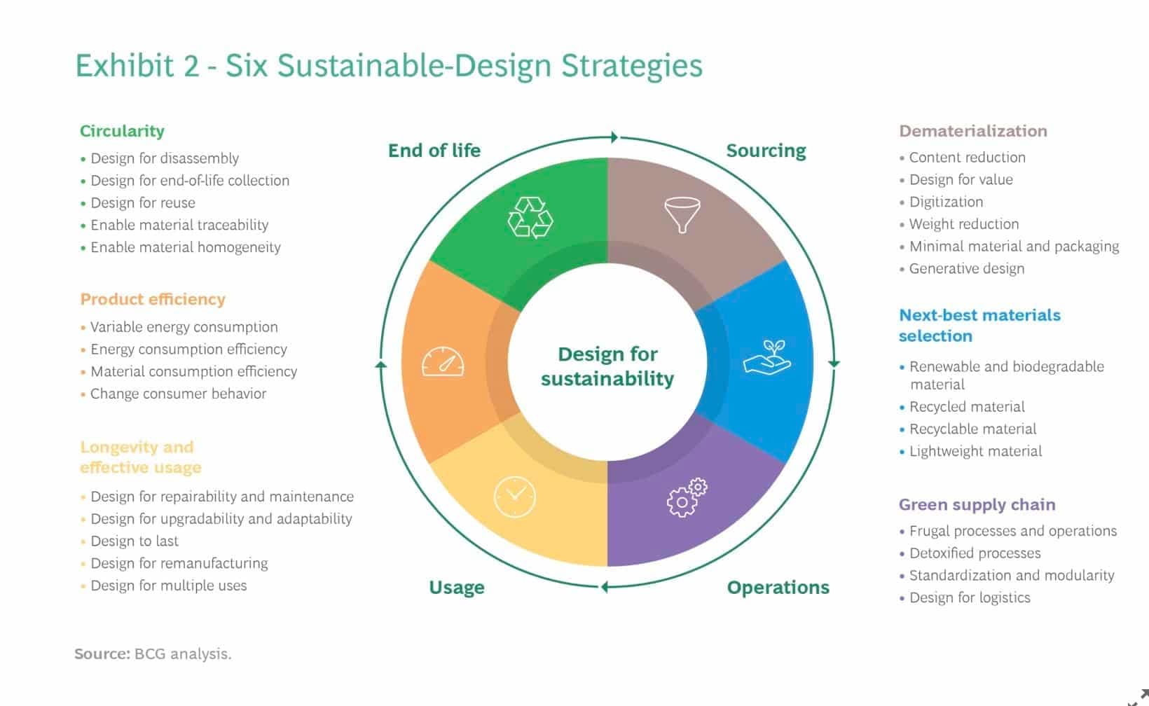
5 techniques to implement sustainable manufacturing
Design products for sustainability
Products can be designed to be environmentally friendly as exemplified by the number of eco-friendly products on the market today. This can be done using recyclable raw materials that live another life and designing for durability.
Design for Disassembly
Design products that can be taken apart easily and be part of a reduce, reuse, recycle loop. This allows parts to be reused instead of ending up in a landfill. This process can reduce consumption of resources and pollution.
Reduce energy consumption of the product
Use components that are energy efficient in building products, build it to last longer so it doesn’t have to be replaced often thereby reducing the carbon footprint involved in building the product. Use raw materials that are bio degradable. Bio degradable materials don’t end up in landfills or in our rivers and oceans. Make your manufacturing facility energy efficient. Use packaging that is lightweight and recyclable.
Lightweighting
Make products with materials that weigh less thus decreasing the overall product weight. Use hollow components where possible for example. This technique is used in automotive and aerospace fields to build lighter cars, trucks and planes that are more energy efficient thereby reducing the carbon footprint.
Eliminate toxic materials
When designing the products eliminate toxic raw materials and use bio degradable or recyclable raw materials instead. This helps the environment by reducing pollution.
Agencies and resources
In the US it is the Environmental Protection Agency or EPA. In India it is the Ministry of Environment, Forest and Climate Change (MoEF) of India and in China it is the Ministry of Ecology and Environment.
EPA India (Aggregator of environmental information and organizations in India)
Conclusion
Sustainable manufacturing is not just a moral imperative; it’s a strategic imperative for businesses aiming for long-term success in a world grappling with environmental challenges. The examples highlighted above underscore the transformative potential of sustainable practices in diverse industries. By embracing sustainability as a guiding principle, manufacturers can pave the way towards a greener, more resilient future for generations to come. Read about the value. proposition of partnering with an EMS in our Ultimate Guide to Electronic Manufacturing Services.
In 1964, Phil Knight started selling imported high-quality, affordable athletic shoes out of his car. He earned $8,000 in his first year. In 2015, Nike earned $30.6 billion. And in April 2016, Phil Knight published his memoir, Shoe Dog, in which he wrote with humour and honesty about the trials and tribulations he – and Nike – faced over that half-century.
Shoe Dog by Phil Knight is an excellent read for any entrepreneur
Shoe Dog is an extremely well-written memoir, an absorbing story full of interesting, eccentric characters and exciting twists. But it also contains plenty of lessons for the entrepreneur. If you are looking for inspiration, motivation and reassurance as you grow your business, I highly recommend you add Shoe Dog to your personal library. I have found it an excellent resource on my own entrepreneurial journey.
Here are eight entrepreneurship lessons I got from Phil Knight’s story.
1. Sometimes, you just have to jump.
At its core, entrepreneurship is a leap of faith. Not all ideas will work out. Evaluate them objectively, discuss with experts, make a plan. But a day will come when you have to stop thinking and take that first step. As Nike’s tagline says, ‘Just do it.’
2. Every day brings its own crisis.
Problems come up all the time – from competitors to new technology, from regulations to finance, from supply issues to weather conditions. The problems of maturing companies are different from those of start-ups. But there’s never a time when all the problems disappear. Accept this and face each challenge with courage.
3. Keep innovating.
Bill Bowerman, an eminent running coach and part of Nike’s story from the time it was still Blue Ribbon Sports, figured out how to reduce the weight of a shoe by one ounce, saving 55 pounds over a mile. That philosophy of iterative improvement has driven Nike ever since. As the pace of technology development gets ever more feverish, embedding the innovative mindset in the DNA of the company is essential to stand out from the competition.
4. Trust is the key.
Five interrelated factors cause a company to lose its way: lack of trust; fear of conflict; lack of commitment; avoidance of accountability; and inattention to results. Entrepreneurship is full of uncertainty. A team that believes in the vision and faces these challenges unitedly is vital to come out of the tough situations. It isn’t that everyone in the company agrees about everything; rather, it is that everyone knows that they all want the company to succeed and views their disagreements in that light. When a company is young and fragile, trust is the glue that holds it together.
5. Failures will happen. Be honest when they do
Knight gives multiple instances of product recalls due to quality issues, mistakes that he made and decisions that, with the benefit of hindsight, could have been better. Nike treated their customers with respect by acknowledging errors, both internally and in public. Nobody is perfect, but when the internal culture of trust is matched by honesty to customers, the circle of trust can buoy a company through some very tough times.
6. Stay humble
One interesting fact is that it was Employee No. 1, Jeff Johnson, who came up with the name ‘Nike’. Throughout the book, Knight praises Johnson, Bowerman, legal counsel Rob Strasser, first COO Bob Woodell and many others, including his wife. Knight rarely mentions his own contributions once the company is more than just a car boot shoe sale. But he was the CEO – how likely is it that he didn’t contribute anything? It’s not an accident that Knight plays down his own role. He knows that success, like sports, is a team effort – and he never forgets to show appreciation for his teammates.
7. Find an outlet for the stress.
Entrepreneurship is demanding. Because the problems never stop coming, you will be tempted to never stop working. But you can’t look after your business if you aren’t around or aren’t in good health. An activity unrelated to work is an excellent way to get a clear, fresh perspective on seemingly insoluble issues. Phil Knight loved running, and running was his outlet. By finding a relief valve and paying attention to your own physical and mental health, you can be energized to keep going, no matter what.
8. Never stop.
For almost the first decade of Nike’s existence, Knight had to work other jobs to support himself. Suppliers ignored or shot down the company’s product ideas. Its first attempt to raise capital was a monumental failure. Advertising flyers got no response. But the team didn’t give up. As an entrepreneur, it’s easy to get disheartened. But if there’s one lesson from Shoe Dog that every entrepreneur should hold on to, it’s this: never stop.
Let everyone else call your idea crazy…just keep going. Don’t stop. Don’t even think about stopping until you get there, and don’t give much thought to where “there” is. Whatever comes, just don’t stop.