A Deep Dive into the PCB Assembly Process
In today’s fast-paced technological landscape, printed circuit boards (PCBs) are the backbone of virtually every electronic device. From smartphones and laptops to medical equipment and industrial machinery, PCBs provide the crucial foundation for electronic components to connect and function. But how does a bare board transform into a fully functional circuit? This is where the PCB assembly process comes in.
PCB Assembly Process is one part of Turnkey PCB Assembly services. Learn more about it in our blog on Turnkey PCB Assembly.
As an experienced Electronics Manufacturing Service (EMS) provider, we understand the intricacies of PCB Assembly. In this blog post, I will take you through a detailed look at the key steps involved in bringing your PCB designs to life.
1. Design and Preparation: Laying the Foundation
Design is the first step in the preparation for the PCB Assembly Process. Check out the Ultimate Guide to EMS Blog to see where Design fits in as part of the core services.
Before any physical assembly can begin, the PCB must be meticulously designed using specialized Computer-Aided Design (CAD) software. This stage involves:
- Schematic Capture: Creating the electrical diagram that outlines the connections between components.
- PCB Layout: Designing the physical arrangement of components on the board, including trace routing, component placement, and layer stack-up.
- Gerber File Generation: Exporting industry-standard files that contain all the necessary information for manufacturing and assembly.
You can learn more about Gerber Files here.
Once the design is finalized, the following preparations are made:
- Bill of Materials (BOM): A comprehensive list of all components required for assembly, including part numbers, quantities, and descriptions.
- Stencil Creation: A thin sheet of metal with precisely cut openings that allow solder paste to be applied to the PCB.
2. Solder Paste Application: Setting the Stage
The first step in the physical PCB Assembly Process is applying solder paste to the bare PCB. This is typically done using a stencil and a screen-printing process.
- The stencil is aligned precisely on top of the PCB.
- Solder paste, a mixture of solder powder and flux, is spread across the stencil.
- A squeegee is used to push the solder paste through the openings in the stencil, depositing it onto the designated pads on the PCB.
This precise application of solder paste is crucial for ensuring reliable electrical connections.
3.Component Placement: Populating the Board
Component placement is the second step in the PCB Assembly Process.
Components are placed onto the PCB. This is usually done using automated pick-and-place machines. These machines need to be programmed to place the components accurately on the PCB. Gerber files are used to do program the pick-and-place machines.
- These machines use vacuum nozzles to pick up components from reels or trays.
- They then accurately position the components onto the corresponding pads on the PCB, where the solder paste holds them in place.
For smaller production runs or boards with through-hole components, manual placement may be used.
4. Soldering: Creating the Connections
This is the third step in the PCB Assembly Process.
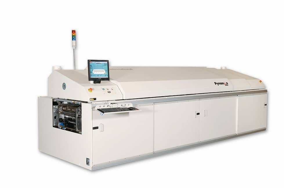
Once all components are placed, the PCB goes through a soldering process to create permanent electrical connections. The most common method is reflow soldering for Surface Mount Technology (SMT) components.
- The PCB is passed through a reflow oven, which precisely controls the temperature to melt the solder paste.
- As the solder melts, it creates strong, reliable connections between the components and the PCB.
- The PCB is then cooled down, solidifying the solder joints.
You can learn more about reflow soldering here.
For through-hole components, wave soldering or manual soldering may be used.

5. Inspection and Testing: Ensuring Quality
This is the fourth step in the PCB Assembly Process.
After soldering, the assembled PCB undergoes rigorous inspection and testing to ensure quality and functionality. This may include:
- Visual Inspection: Checking for any defects such as misplaced components, solder bridges, or insufficient solder.
- Automated Optical Inspection (AOI): Using cameras and software to automatically detect defects.
- X-ray Inspection: Examining solder joints beneath components like Ball Grid Arrays (BGAs).
- In-Circuit Testing (ICT): Using test probes to verify the electrical performance of the circuit.
- Functional Testing: Testing the PCB in a simulated or real-world environment to ensure it meets the design specifications.
6. Cleaning and Finishing: Final Touches
This is the fifth step in the PCB Assembly Process.
In some cases, the assembled PCB may need to be cleaned to remove any flux residue. This is typically done using deionized water or specialized cleaning solutions.
Additional finishing processes may include:
- Conformal Coating: Applying a protective layer to protect the PCB from environmental factors such as moisture and dust.
Partner with a Reliable EMS Provider
The PCB assembly process is a complex and multifaceted process that requires expertise, precision, and state-of-the-art equipment. Partnering with a reliable EMS provider like us can ensure the highest quality and efficiency for your PCB assembly needs.
We offer a comprehensive range of services, including:
- Prototype Assembly: Quick-turnaround assembly for initial prototypes.
- Low-Volume and High-Volume Production: Scalable assembly solutions to meet your production needs.
- Turnkey Solutions: Complete end-to-end services, from component procurement to final assembly and testing.
By choosing us as your EMS partner, you can focus on your core competencies while we take care of your PCB assembly needs. Email us at [email protected] today to learn more about how we can help bring your electronic innovations to life.