• 35, 1st Main Rd, Munireddy layout, Bandepalya, Garvebhavi Palya, Bengaluru, 560068

Social

Educational Options to enter EMS Industry

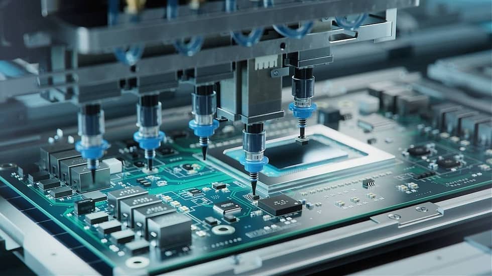
The electronics manufacturing services (EMS) industry in India has been growing rapidly over the past few years, and the growth rate is expected to continue in the future. According to a report by Research And Markets, the Indian EMS market was valued at USD 35.4 billion in 2020, and it is expected to grow at a compound annual growth rate (CAGR) of 21.8% from 2021 to 2026. Any growing industry also needs skilled people to aid its growth.

Career Options for EMS

A good vocational education program is a great way to start in the EMS industry

An electronics manufacturing services (EMS) company typically employs a range of professionals with different skills and expertise.

  • Manufacturing engineers responsible for optimising the manufacturing process and designing production systems.
  • Quality Control Engineers who inspect products, conduct tests and implement quality control procedures to ensure that products are manufactured to specifications.
  • Supply Chain Managers and Logistics Co-ordinators who work with suppliers to ensure on time delivery and manage inventory levels for production schedules.
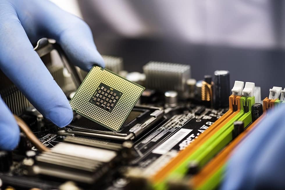
  • Assemblers / Technicians: This role is the backbone of the industry and many who move on to quality control and supply chain management, make their start as assemblers / technicians.

Getting a start in this sunrise industry requires a combination of education and practical training. For students or even those who are mid-career, wondering what will help you, here are a few thing to consider:

  1. Get a Technical degree: This is the best option for students who are still planning their education. Pursuing a degree in electrical engineering, electronics engineering, or a related technical field can provide a strong foundation for a career in EMS. These degree programs typically cover topics such as circuit design, digital electronics, microcontrollers, and power electronics.
  2. Join a Vocational training program: Vocational training programs, such as those offered by ITI’s or trade specific orgalisations like Electronics Sector Skill Council, can provide hands-on training in electronics manufacturing. These programs may cover topics such as soldering, PCB assembly, and quality control. Vocational training programs can sometimes be regarded as less prestigious but there is no parallel to the practical learning they offer and their grounded and quick start to careers. 
  3. Certifications: Obtaining industry certifications, such as IPC-A-610 (Acceptability of Electronic Assemblies) and IPC-J-STD-001 (Requirements for Soldered Electrical and Electronic Assemblies), can demonstrate expertise in specific areas of electronics manufacturing and can be very valuable.
  4. Internships or apprenticeships: Participating in an internship or apprenticeship program with an EMS company can provide valuable on-the-job training and help you gain practical experience in electronics manufacturing. Podrain has been offering paid internships since inception. Some of our interns go back to studying but many move on to working with us or other peers in the EMS industry

Overall, a combination of technical education, hands-on training, and industry certifications can help prepare you for a successful career in Electronics Manufacturing Services.

For more information on careers at Podrain write check our website and write to us as [email protected]

Note: Post generated with assistance from ChatGPT3

Read More

Better Waste Management

Modern manufacturing practices pay close attention to their environmental impact. Failure to do so has legal and regulatory implications as well as marketing ones: suppliers’ ‘green’ credentials are frequently a criterion for selection.

The electronics industry – and the PCB industry in particular – uses many metals and processes that create large quantities of ecologically harmful waste. Some metals are dangerous if not disposed of properly, and many that can be reused are often squandered in landfills due to poor waste management practices.

Better Waste Management Practices are the need of the hour

Waste in the PCB industry

A number of materials go into the assembly of a PCB. Most PCBs use resin epoxy, phenolic resin, fibreglass and copper foil. Depending on the complexity of the circuitry in the design, metals including copper, aluminium and iron, and several alloys, may be used. At the end of its life, a PCB that is discarded means those metals and alloys go to waste.

On average, a PCB contains approximately 70% non-metallic and 30% metallic material: organic materials, chemical residuals, heavy metals and high-grade precious metals including palladium, silver, gold and copper. It is estimated that up to 7% of the world’s gold supply may be found in e-waste.

But it is not just the product itself that contains potentially wasted value. A great deal of waste is generated during the manufacturing process itself. For example, during production a PCB must be rinsed several times, leading to water contamination by chemicals and metals, and the release of some acidic emissions into the air.

In February 2003, the European Union issued the Restriction of Hazardous Substances Directive, or RoHS. This directive states that PCB manufacturers wishing to operate in or sell to EU entities may not use six hazardous substances in any stage of their production process – lead, mercury, cadmium, hexavalent chromium, and the fire retardants polybrominated biphenyls and polybrominated diphenyl ether. As the EU is a large and influential market, over the years, PCB production around the globe has begun to comply with the RoHS regardless of where the customer is.

Also in 2003, the first WEEE (Waste Electrical and Electronic Equipment) Directive was introduced, regulating the recycling of electronic waste. Under WEEE, companies that manufacture, distribute or sell electrical and electronic equipment have an obligation to treat it responsibly.

The WEEE became more stringent in 2008 and the RoHS in 2011, increasing the amount of e-waste that is required to be treated and reducing the amount that can be disposed of.

How can waste be reduced?

There are several methods by which PCB manufacturers can address the challenge of managing their waste and minimizing their environmental impact.

Product substitution.

Several alternatives may be substituted for harmful items, especially for supplementary processes like packaging, where sustainable materials are available, which can make an immediate impact on the quantum and composition of waste, and which are relatively easily to obtain and adopt.

Replacement of hazardous materials.

 In advanced manufacturing, new techniques, tools and materials are being introduced all the time. For example, when cleaning and preparing PCB surfaces, changes to the materials used, the safety precautions taken and the processes themselves can yield significant results. By using abrasive cleaning and non-chelated materials, manufacturers can reduce the amount of hazardous waste produced. A cascade cleaning system cuts down on the generation of nitric acid as a waste product. It should be noted that cascade systems are not new – for several decades, they have been used to clean machine parts in the heavy electrical industry. Customizing cascade systems for PCB manufacturing is a logical next step.

Material reuse or recycling. 

Some of the materials used in the production of a PCB can be put back into the production process. Copper from the edge, tin and lead-tin from the solder dross are examples of this. By reusing parts, the process also uses less water. Copper oxide can be used to reduce the reliance on copper hydroxide, which is harmful to the human respiratory system.

Material recovery and segregation.

 By joining in or setting up a well-thought-out recycling process, manufacturers can turn waste back into raw material, or supplement their earnings by selling their recovered materials to other industries. Alloys and metals are valuable and can be reused several times, reducing the amount of waste generated and the PCB manufacturer’s dependence on being able to source new materials on time and at the right price.

Traditional PCB recycling involves dismantling the boards, crushing them and physically separating them using magnetic or high-voltage electrostatic methods. This approach is relatively cheap and enables the recovery of metallic components, though it does not solve the problem of segregating heavy metal elements from high-grade precious metals.

Thermal or chemical recycling can obtain purified metals, is much more efficient and has the potential for a much greater economic return. However, the high processing temperatures or high-pressure requirements can cause hazardous fumes, thus creating a new problem while resolving the existing one.

Podrain has tied up with a reliable, pollution control board certified partner for waste disposal. We also return materials and components (unused or even partially working) to our customers so that they can be reused at their end.

We value sustainability and even if we move to an inventory led model we will hope to find solutions that will continue to keep our manufacturing sustainable. 

Read More

Factory Layout – What are the Options

In my previous post we covered what to consider for factory location. Having selected a location in which to set up a factory, the next question is how to lay it out.

Factory layout refers to the arrangement of physical facilities so as to have the quickest flow at the lowest cost and with the least amount of handling in processing from the receipt of material to the dispatch of the finished product. The aim is to allocate and arrange space and equipment to minimise operating costs.

As with location selection, factory layout is a long-term commitment. To optimise the relationship between output, floor area and manufacturing process, an efficient layout must achieve multiple objectives simultaneously:

  1. The proper and efficient use of the available floor space
  2. Work should proceed from one point to the next without delay
  3. Adequate production capacity and flexibility, including potential to expand, at least in the short- to medium term
  4. Lower material handling costs
  5. Employee health, safety, accident and injury prevention
  6. Efficient labour and equipment utilization and productivity
  7. Maintaining quality standards, managing waste and storing inventory
  8. Ease of supervision, and control
  9. Plant and equipment maintenance
  10. Complying with local regulations

Factory Layout Options

There is no one-size-fits-all option. Each factory, location and industry is unique, though the basic principles remain the same. 

For small and medium manufacturing units, there are three main layout options, for which the main pros and cons are laid out below:

Product (Line) Layout

Equipment is arranged in a single line determined by the sequence of operations in this layout. Advantages are that it is low cost, operations are smooth and have continuity. The production control process is also simpler. However, the layout lacks flexibility. One process breakdown can bring the whole factory to a halt. 

This layout is best suited for mass production where the process is repetitive, demand is stable and material availability is reliable. 

Podrain expects to use this design for our larger ‘volume production’ factory. 

Process Layout

Sub-process equipment and staff are grouped together in this layout. This is flexible and adapts fast to changes in volume and product variety. It’s also possible to ensure specialised supervision where needed and ensure high utilisation. However, more skilled labour is needed and production controls need to be strong to avoid time lags and inventory accumulation. 

This layout is best suited for non-standard product lines, smaller quantities and where frequent changes to design may be needed. Podrain currently uses this layout in its prototype and small batch manufacturing facility. 

Combined Layout

This blends the product layout and process layout where some steps of production are laid out by product line and others have sub process equipment and staff grouped together. this is a very complicated layout to design. When done right, it can offer efficiency and better production controls. However even a small error can lead to being stuck with bottlenecks in the production process. It’s typically used in very large manufacturing organisations for FMCG items. 

Single-Storey vs. Multi-Storey Factory

Land is scarce, and suitable land is scarcer still. So, having selected a location and figured out the plant layout, one is left with the decision of a single-storey versus a multi-storey building.

Single-Storey Building -Advantages:

  • Greater floor loads, no structural strength needed to support upper storeys
  • Lower noise transmission and building vibration
  • Ease and lower costs of building and expansion
  • Natural light and ventilation
  • Higher floor area usable for processing – no stairwells, lifts, shafts, etc.
  • Concentration of service facilities centrally yields lower operating costs
  • More efficient layout and material handling, product routing
  • Lower cost of supervision

Multi-Storey Building – Advantages: 

  • More efficient utilization of land area, and smaller land area requirements
  • Temperature management costs are significantly lower
  • Greater structural strength, higher construction quality, fireproof and longer-lasting
  • Upper storeys dust-free, especially for precision manufacturing operations
  • Downward chutes are cost-effective for material movement
  • Compact, more efficient layouts – though there is a limit to the benefit of this

Whether single- or multi-storey factories are more economical to build and operate per square foot of usable floor space is hard to determine. Local and regional considerations regarding regulations and land prices may play a significant role and costs may vary over the course of time. For example, our Bangalore factory is a multi-storey facility. While production control is a little more difficult, land availability at a central location in the city is a key factor in our choice. 

In conclusion, siting, designing and building a plant that’s conducive to business success is all about balancing the trade-offs between costs, time, complexity and benefits in pursuit of the goals of the company.

Read More

Factory Location: How to make a choice

India

India

Entrepreneurship is all about making decisions and one of the key decisions every manufacturing entrepreneur faces is the best location and layout for the plant or factory. Should it be in a city, semi-urban or industrial area? Is proximity to an employee pool, educational centres and public transport important? What about public utilities? Taxation and incentives?  Which amenities are likely to be most vital to success?

We’ve been thinking about this at Podrain and went back to basics on it.

Plant location is a strategic decision that  is nearly impossible to change without incurring considerable losses. The ideal location is one that minimizes the cost of production, supports a large market share, maximises social benefit and eliminates risk. Locational analysis that takes into account demographics, trade area (availability of and access to customers), competitive, economic and traffic analyses and can help determine the right location.

A location in which some costs are higher may still be the best choice if it maximises net advantage, i.e., its overall unit cost of production is lowest.

Here are some things we are considering when selecting a suitable location for a factory:

  1. Natural or climactic conditions
  2. Cost of land or land lease
  3. Availability and access to raw material
  4. Transport costs – inward, to bring in raw material, and outward, to sell or distribute finished products
  5. Availability and access to market
  6. Availability and access to infrastructure – developed industrial sheds, link roads, transport hubs, public utilities, civic amenities, means of communication
  7. Availability and access to both skilled and unskilled labour, as required, and local labour rates
  8. Availability and access to banking and financial institutions
  9. Safety and security of the plant, its workers and its assets
  10. Government and regulatory environment – positive and negative incentives, including cheaper utilities, tax relief, liberal local labour laws, pollution control and waste disposal regulations, among others
  11. Personal reasons, such as being close to family, familiarity with a particular place, or a network of known associates whom we can call upon for financial, operational and emotional support. This isn’t intuitive to admit but it’s really important to have a good support system.

Not all these considerations carry equal weight. For example, government incentives cannot compensate for poor public infrastructure. Running costs at a plant can contribute significantly to the overall cost of manufacturing, and poor location selection can cause a business to fail as its growth and efficiency are constrained.

MSMEs like us often do not have the financial or operational capacity to compensate for the shortcomings of public infrastructure , so our ability to adjust to an unsupportive environment is extremely low, particularly in the early stages of the manufacturing journey.

Is there something else we should include? What is your experience. Do write to us or add your comments to let us know.

Read More

Quality testing for prototypes

In PCB manufacturing, repeatability and consistent quality are critical – whether for large-scale production, small batches or prototypes.

Skilled and experienced technicians can and do create excellent work, but relying on individuals to establish, deliver and sustain top-quality results is risky. Programming Automatic Inspection Machines and processes is expensive, time-consuming and not always practicable, especially when prototyping.

Testing

Testing

Prototype QC needs to ensure that the design will work; that it is safe, and meets certain standards of quality and reliability; that it performs to expectations; and that it addresses its purpose.

Small batch PCBs have some rather unique attributes:

  • High Mix, Low Volume (HMLV). It’s likely that the PCB manufacturer builds several board designs in this environment to ensure efficient use of their production infrastructure.
  • Higher performance, reliability and quality requirements. Small batch and prototype PCBs are often intended for critical applications where more stringent IPC standards apply, like aerospace, automotive safety or medical devices. Quality and reliability expectations can be significantly higher for these critical system applications.
  • Complex designs. Prototypes are created to solve specialized and often complicated challenges, which means their designs are complex, requiring atypical manufacturing processes

How to ensure the best quality standards for prototypes and small batches

  • In-circuit testing (ICT). Provides a reliable, high-fault coverage verification method for the majority of PCB assembly electronic components that’s free of human error. It’s great for big assemblies or ball grid arrays and after assembly.
  • Short circuit testing. The main cause of PCB prototype defects is a short circuit between its larger components. For example, a fastener between two proximate pins can damage the microcontroller by triggering a short. It is vital to gauge the impedance each voltage node to the ground. Faulty components or incorrect soldering can cause components to overheat.
  • Flying probe test. A practical, cost-effective technique for prototypes and small batches that tests PCB probes from one spot to another, looking for singular issues in the circuit – shorts, capacitance, resistance, inductance, opens and problems with diodes.
  • x-ray inspection. As the prototype is being manufactured, an x-ray technician runs tests to locate defects, looking for elements that may be hard to discern with the naked eye – for example, joined connections, internal traces or barrels.
  • Functional testing. The #1 criterion for a prototype’s success is, “Does it work?” Performing a functional test requires the parameters for ‘success’ to be clearly defined. Functional testing takes a long time, because it simulates the real-life environment in which the prototype is expected to work. But in terms of long-term value, it’s worth doing. A great deal of money and time can be saved by identifying potential operational pitfalls and eliminating them at the design stage.
  • Burn-in testing. Intended to identify failures early and initiate load capacity. Burn-in testing helps identify potential dangers relating to power being pushed through the electronic components for extended periods of time. One must keep in mind that individual prototypes may be partially or even completely damaged by a rigorous burn-in test, and the test’s utility to prototype QC should be decided based on the destination application of the PCB.
  • Automated optical inspection testing (AOI). Camera-based visual inspection to identify issues that may emerge on the board during the preliminary phase of assembly. It’s wisest not to rely entirely on AOI, but to complement it with an ICT or flying probe for more accurate QC results.
  • Inverted polarity testing. The more manual assembly, the higher the risk of human error. The simple act of ensuring that each individual component is set up based on its polarity can prevent the complex and delicate components of your prototype being badly damaged. Protection diodes can protect PCBs but add to their power consumed.
  • Populated components testing. A simple BOM cross-check to ensure that the components selected fit the board design can save investigative time and effort later in the process.

Several other QC approaches, including tests for PCB contamination, solderability and peeling; micro-sectioning analysis; and time-domain reflectometers, can identify faults or be used in combination with those discussed above, like ICTs and flying probes.

Choose the right QC test(s) for your prototype

It begins with clearly defining the purpose and desired performance levels of the PCB; weighing the pros and cons of the available tests – which include costs, time required, destructive vs. non-destructive; and always keeping in mind, especially when prototyping, that the design-test loop can flex and adapt as the product design is iteratively perfected.

It’s always a good idea to partner with a manufacturer who is committed to the best quality; has documented and traceable processes; has the necessary quality and classification standard certifications; is experienced at HMLV manufacturing; and leverages technology to ensure high-quality, repeatable results.

Podrain collaborates closely with its clients when prototyping and producing small batches, and meets the highest quality and classification standards. We advise clients on the right mix of testing to ensure that their prototype PCBs meet the final test of quality – sustained, reliable, top-level performance in the field.

Read More

Complex assemblies – some samples

Telit ME910 / LE910

Part number: ME910 / LE910
Telit ME910 / LE910
  • Part Number: ME910 / LE910
  • Make: TELIT
  • Dimensions: 28.2 X 28.2 X 2.2 MM
  • 4G LTE, CAT 1, 4
  • Mobile IoT 3GPP REL 13, 14 – LTE CAT M1, NB1, NB2 
  • 3G and 2G Series
  • Voice Capable Variants – Volte, Analog, and Digital Audio
  • Certified with Regulatory Bodies and Mobile Operators Worldwide
  • Multiple I/O
  • Optional GNSS

Digi International : CC-WMX-JN58-NE

  • Part Number: •CC-WMX-JN58-NE
  • Make: Digi International
  • Dimensions : 29mm X 29mm X 3.5mm
  • Description : Bluetooth, Wi-Fi, 802.11A/B/G/N/AC, Bluetooth v4.0 Transceiver Module 528 mhz  Surface Mount

Quectal: EG95EXGA-128-SGNS

Quectal: EG95EXGA-128-SGNS
  • Part Number: EG95EXGA-128-SGNS
  • Make: Quectel
  • Dimensions: 29mm X 25mm X 2.3mm
  • Description: Cellular, Navigation Beidou, Edge, Galileo, Blonass, GPS, GNSS, GPRS, GSM, HSPA+, LTE, UMTS, WCDMA Transceiver Module – Antenna not included Surface Mount

Telit: GE310-GNSS

Telit: GE310-GNSS

Part Number: GE310-GNSS

Make: TELIT

Dimensions: 18mm X 15mm X 2.2mm

Description:  Automated Manufacturing Process Friendly. Miniature and Futureproof footprint. BT 4.0 Transceiver. GPS, GLONASS, Galileo and Beidou navigation, Ideal solution for applications such as asset management, utilities, and telematics. Battery-friendly operation with 2.8V GPIOS.

Quectel: EG91NAFB-512-SGNS

Quectel: EG91NAFB-512-SGNS
  • Part Number: EG91NAFB-512-SGNS
  • Make: QUECTEL
  • Dimensions: 29mm X 25mm X 2.3mm
  • Description: Cellular Navigation on Beidou, Galileo, Glonass, GPS, GNSS, LTE, UMTS, WCDMA. Transceiver module- Antenna not included surface mount

Honeywell: LGA_299_35MMX35MM_BETTER_SOM

Honeywell: LGA_299_35MMX35MM_BETTER_SOM
  • Part Number: LGA_299_35MMX35MM_BETTER_SOM
  • Make: Honeywell International Inc.
  • Dimensions: 35mm X 35mm X 6mm
  • Description: SOM , I.MX6 SOLOX-2 , 4GBYTE EMMCFLASH , 1GBYTE DDR3L

New Technologies Inc: A-365-MQ-A00

  • Part Number: A-365-MQ-A00
  • Make: New Technologies Inc
  • Dimensions: 22.5mm X 15.05mm X 1.13mm
  • Description:  The A-365-MQ Fingerprint sensor is a fingerprint scanner in an LGA Style package. The sensor is based on capacitative contact technology with hardened surface and enhanced ESD immunity.
Read More

complex assemblies

Metal BGA

Electronics have become essential to daily life. Everything from refrigerators to military aircraft contains electronics. Today’s critical advanced assembly challenges mainly fall into three categories: performance, usability and productivity. To build and visualise product designs quickly and economically, engineers must address all these challenges.

On the other hand, manufacturing techniques are becoming more advanced and aesthetics are increasingly in demand. Project lifecycles and budgets are constrained. Sometimes, these constraints mean that DFM standards are overlooked in PCB design. For example, if the PCB has to fit in a box of fixed dimensions, the PCB design has to be tweaked accordingly. Or, components with different reflow profiles may be used on the same sid

Newer design houses or inexperienced engineers and designers may be prone to these mistakes. But not validating designs with tool and industry standards is bad practice. Here are just a few examples:

Pad mismatch

 If the copper termination pad separates partially or completely from the board, it can be hard to identify the fault; the pad may look intact as the solder usually remains attached to the component. The cause is usually mechanical strain that begins during testing, manufacturing, vibration while being transported or even when connectors are attached. PCB performance is impaired and performance is inconsistent. Extensive or even destructive testing may be required to positively identify the cause. Podrain follows a painstaking process to minimise the risk of damage from pad mismatch at each step.

No silkscreen. 

The silkscreen does not impact the electrical functionality of a PCB, but it is still extremely valuable as it provides essential information when assembling the PCB. It provides simple visual feedback that helps to catch deeper problems. It is not merely for aesthetic purposes. It is information that should not be separated from the board. Unique ID numbers, warning symbols, certifications etc. should be displayed on the board. At Podrain, we treat correct and comprehensive silkscreens as an integral part of the PCB.

THT vs. SMT components. 

When SMTs were developed in the 1980s they were expected to completely replace THTs. But THTs and SMTs are not always interchangeable. THTs offer reliable and useful in test and prototyping applications where frequent manual adjustments and replacements are needed. But SMTs are almost always more efficient and cost-effective. Podrain’s extensive experience in a wide range of applications gives us the expertise to know which type of components to use for a given project.

Incorrect polarity marking. 

To prevent polarised component packages from being inverted during assembly machine setup or manual soldering, accurate polarity marking is critical. It is only necessary for land patterns that have a specific rotation during assembly. Incorrect polarity markings can cause equipment damage, short-circuiting, serious injury, fires or even explosions. Podrain follows stringent Post Assembly Inspection Process protocols to visually validate that assembly insertion is done correctly

Incorrect component separation. 

Most designers are used to PCB clearance rules for spacing between traces in a single layer. However, many design houses overlook PCB clearance between layers. Today’s circuit designs often involve a single PCB with power and controls on the same substrate. This may put high-voltage traces close to low-voltage signals, creating a risk of arcing. The resulting sparks can permanently damage the port of the low-voltage component. Podrain designers and engineers keep ourselves up to date on the latest IPC-2221B design standards to ensure optimum manufacturability with minimum risk.

Podrain’s customers have brought us some interesting design challenges.

A top manufacturer of electric vehicle charging stations found that the PCBA yield was below 90%, lower than expected. The company approached Podrain to investigate. The issue was all the more challenging because the assembly was ROHS. Planning and finding the right profile, especially on a PCB that uses BGA + LGA, is an art.  By devoting our experienced people to solve this, we iterated through a range of 11 temperature profiles in a reflow oven within just 2 days to find the solution.

Another customer set us the challenge of setting the right profile for a board designed with a heavy BGA connector having multiple ceramic BGAs, including micro BGAs, on a 2mm thick PCB. The issue is these kind of connectors use very high temperature for soldering. 265 degree Celsius plus is needed for soldering but a normal BGA can tolerate only 245 to 255 degree Celsius. We designed and conducted multiple trials by changing the solder paste for each profile. After 15-20 trials supported by some fixtures, we were able to determine the best profile for the customer’s board.

Podrain has solved many such complex assembly design challenges for our customers.

Read More

The Art of Quick Turn Prototype Manufacture – Some learnings

As a PCB assembly and manufacturing unit, we face several challenges in ensuring we can meet the turnaround time our clients ask for while still delivering a quality product. This is a short post on the challenges we face and how we solve them.

6 M framework based thinking helped Podrain find solutions for quick turnaround manufacture

Managing Part Availability Delays

Every manufacturing organization has dealt with issues in this area. The critical part is held up in customs. A normally reliable supplier doesn’t have stock just now. The wrong part got shipped. The list of such issues can be long. Our clients purchase the parts for us in most cases because we are a “job-work” oriented partner, but there are many occasions when the part isn’t available on time but the end date to finish the manufacture is the same!

We’ve seen clients work hard through the day and the part reaches us at the end of the regular workday. We have adapted by having a 3 shift operation in place so that we can take up the order manufacture at any time and ensure client timelines are met. We also ensure that our strongest team members are available on the late shift. It can be tough working late at night on an important order and we put our toughest people on the job to make sure it gets done right.

There are some consumables, that we must order and here we invest in supplier relationships. Our stencil suppliers, for instance, deliver within a few hours because they know they can trust our volume commitments and payment cycles.  

Kit Condition Checks First

For larger clients who have their own kitting teams, 99% of the kits arrive in good condition and we can start manufacture immediately. However, many of our clients are startups or design houses that are still experimenting. The parts are directly shipped to us without kitting checks at the client’s end. 

We solve this by frontloading our effort in checking kits. Where other manufacturers would ask two people to run kit checks, we allocate 6 people. And we work with the client to solve for deficiencies right away – if there is a part shortfall can we run a smaller batch? Is there additional testing we can do on a smaller batch, while we wait? Is there an alternate part or source we have seen that we can connect them to? We work flexibly with our partners to ensure their goal is met.

Data Package Standardization

In the past when we accepted all client data packages as-is, we would spend a day verifying the documents – gerbers, assembly drawings, additional assembly instructions, etc. – and then mapping them to our process to ensure there were no misses. Working with our clients we realized many of them were flexible on giving us this information in a format that we requested. This saves us time and ensures we can follow a Total Quality Management process even within a 48 or 72-hour manufacturing turn. 

We’ve used the 6 M framework – Manpower, Method, Machine, Material, Milieu and Measurement to think through problems and find some of these solutions. I highly recommend this to anyone working in Manufacturing or even in other industries.  

That’s it for this month. I’ll write again with more of our learnings next month. 

If you want to know more about Podrain and our electronics manufacturing services contact us and we will get back to you at the earliest

Read More
Solder Paste

Solder Paste Choice

Solder paste printing attaches surface mount devices to printed circuit boards. Over 70% of Surface Mount Technology defects are driven by solder problems.* The choice of solder paste can make a huge difference. As devices and their components become smaller, the solder connections are also correspondingly finer. Its hard to fill apertures for these small devices with coarser type 3 solder paste. Type 2 solder paste is almost never used on Printed Circuit Boards. Rather, it features in power and industrial products where the chip package is bigger.  


Until 2017, India had easy access only to type 3 solder paste which has 25-45 microns powder size. While it is possible to use type 3 solder paste for lead pitch between 0.3mm and 0.02mm , the reliability and durability of the boards reduces. Type 4 solder paste yields better results in our experience. We also use a Solder Paste Inspection system to ensure the right amount has been used.


Podrain has been sourcing and utilising type 4 solder paste, even though it entails a 20%-30% higher cost for the past 4 years. Now, we see an across the industry move to Type 4 solder paste  and even the manufacture of Type 3 solder paste is coming down. We are currently evaluating switching to type 5 solder paste which has a powder size of 15-25 microns for components that need to go on the smallest PCB’s. 


So when you are looking for a provider to make your PCBA’s, go beyond looking at the machines on the assembly line, and ask what solder paste is used. 


*Biemans. 2011. “5D solder paste inspection merits beyond 3D technology.” Global SMT and Packaging 8-13 

References

https://blog.gotopac.com/2020/03/13/solder-paste-types-powder-sizes-for-smt-dispensing/

https://scholarworks.rit.edu/cgi/viewcontent.cgi?article=10208&context=theses


Read More